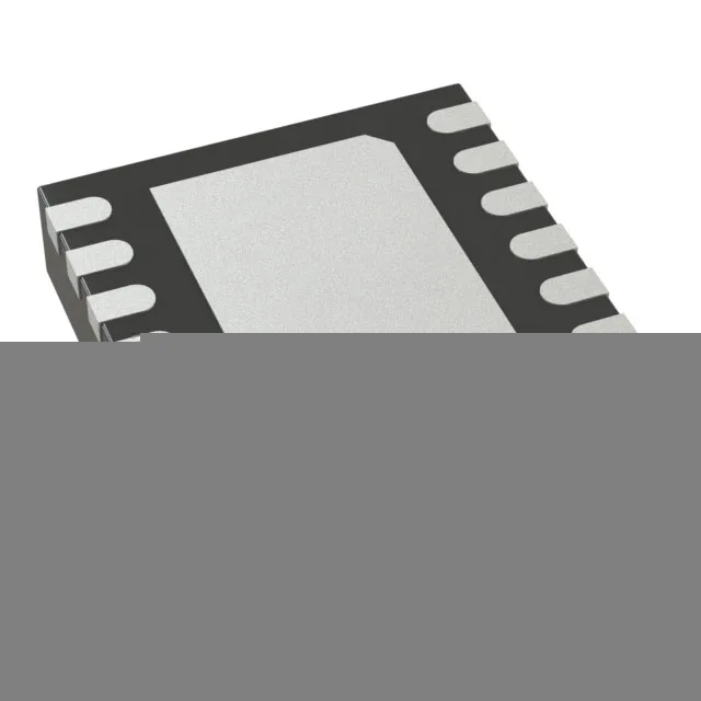
Analog Devices LTC6957IDD-4#PBF — Clock & Timing ICs

LTC6957IDD-4#PBF Analog Devices Fanout Buffer, 300 MHz

MPNLTC6957IDD-4#PBF
End of Life

Analog Devices LTC6957IDD-4#PBF, Fanout Buffer (Distribution), 1:2 ratio, 300 MHz max frequency, CMOS output, 3.15V–3.45V supply, 12-WFDFN exposed pad package.

$10.82Ref. price · indicative, final on quote
Packaging12-WFDFN Exposed Pad
RoHSROHS3 Compliant
Independent supplier — new & surplus stockAuthenticity-screened · ESD-safe packingListing updated Aug 2026

Specifications

LTC6957IDD-4#PBF specifications
ParameterValue
TypeFanout Buffer (Distribution)
MountingSurface Mount
Supply voltage3.15V ~ 3.45V
Frequency - max300 MHz
Operating temperature-40°C ~ 85°C
InputCML, CMOS, LVDS, LVPECL
OutputCMOS
PackageTube
Case12-WFDFN Exposed Pad
Number of circuits1
Ratio - Input:Output1:2
Differential - Input:OutputYes/No

Product details

Clock buffer selection for multi-standard inputs

The LTC6957IDD-4#PBF is a single-channel fanout buffer that accepts CML, CMOS, LVDS, or LVPECL inputs and delivers a single-ended CMOS output at up to 300 MHz. The 1:2 fanout ratio means one input drives two output copies, useful for splitting a clock to two loads without adding a separate distribution IC.

The buffer operates from a 3.15V to 3.45V supply — a 3.3V rail with ±5% regulation is fine, but a rail with high ripple or droop under load may push the buffer out of its specified range.

Analog Devices lists the LTC6957IDD-4#PBF as Active in production.

Frequently asked questions

Will LTC6957IDD-4#PBF drop into a board designed for LTC6957IDD-3#PBF without rewiring?

Both parts share the same package (12-DFN 3×3 mm), supply voltage range, and pinout — the -3 suffix outputs CMOS as well. The -4 variant is functionally identical for a CMOS-output design; no board respin is needed. Confirm the input signal type (CML, CMOS, LVDS, LVPECL) matches your source.