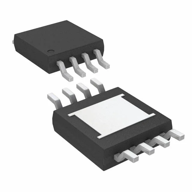
Half-bridge N-FET driver for 48V–72V bus converters
The LTC4444MPMS8E#PBF is a half-bridge gate driver from Analog Devices designed to drive two N-channel MOSFETs in a high-side / low-side configuration. It delivers 2.5 A peak source and 3 A peak sink current at the gate, with 8 ns rise and 5 ns fall times typical — fast enough for switching frequencies above 500 kHz in synchronous buck or full-bridge topologies. The bootstrap supply handles up to 114 V on the high side, making this driver a fit for 48 V to 72 V input bus converters, telecom rectifiers, and intermediate bus architectures. The supply rail itself runs from 7.2 V to 13.5 V — a standard 12 V gate-drive bias rail is ideal.
Military temp range and package thermal path
Rated for -55°C to 150°C junction temperature, this is the military-grade (MP) suffix — suitable for avionics, downhole instrumentation, or engine-bay power stages where the ambient exceeds 125°C. The 8-MSOP-EP exposed pad must be soldered to a PCB copper plane to keep the junction below 150°C at full 3 A sink current. Logic input thresholds are 1.85 V (VIL) and 3.25 V (VIH) — the driver is 3.3 V logic compatible. A 1.8 V logic source may not reliably reach the VIH threshold; a level shifter or pull-up resistor to the driver supply is recommended in that case.
Independent channels with non-inverting inputs
The two driver channels operate independently, each with a non-inverting input — a logic high on the respective input turns on that output. There is no internal dead-time or cross-conduction prevention; the dead-time must be generated externally in the PWM controller or FPGA.
Active lifecycle and compliance documentation
Packaging is tube (bulk), not tape-and-reel — order quantities are typically multiples of the tube count. For automated pick-and-place, verify that the tube orientation matches the feeder requirements.