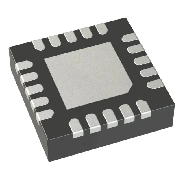
Analog Devices LTC3562EUD#PBF — Logic ICs

LTC3562EUD#PBF Quad Buck Regulator, 2.25 MHz, 400mA/600mA

MPNLTC3562EUD#PBF
End of Life

Analog Devices LTC3562EUD#PBF, Quad Step-Down Buck Regulator, Adjustable Output, 2.7V to 5.5V Input, 400mA/600mA Output, 2.25MHz Switching, 20-WFQFN Exposed Pad, -40°C to 85°C, Tube.

$10.29Ref. price · indicative, final on quote
Packaging20-WFQFN Exposed Pad
RoHSROHS3 Compliant
Sourced new & surplus through independent channelsAuthenticity-screened · ESD-safe packingListing updated Aug 2026

Specifications

LTC3562EUD#PBF specifications
ParameterValue
Output typeAdjustable (Programmable)
MountingSurface Mount
Voltage - input5.5V
Voltage - output0.8V (3.78V)
Voltage - output (Min (Fixed))0.425V (0.6V)
Output current400mA, 600mA
Frequency2.25MHz
I/O channels4
Operating temperature-40°C ~ 85°C (TA)
PackageTube
FunctionStep-Down
TopologyBuck
Case20-WFQFN Exposed Pad
Output configurationPositive
Synchronous rectifierYes

Product details

Four 400mA/600mA rails from a single 5.5 V input

The LTC3562EUD#PBF is a quad-output synchronous buck regulator from Analog Devices that packs four independent step-down converters into a 20-pin QFN package measuring 3 mm by 3 mm. Each of the four outputs delivers either 400 mA or 600 mA, with the higher-current channel typically assigned to the core rail and the lower-current channels to I/O or auxiliary supplies. The 2.25 MHz switching frequency keeps the inductor values around 1 µH to 2.2 µH, which saves board area in space-constrained portable and battery-powered designs. Each output is adjustable down to 0.425 V and up to 3.78 V, which spans the common core voltages for FPGAs, SoCs, and low-voltage digital logic as well as 1.8 V, 2.5 V, and 3.3 V I/O rails.

The part ships in Tube form. The ROHS3 compliance is consistent with current lead-free assembly requirements; no special handling beyond standard MSL precautions is called out in the listing.

Output voltage flexibility for multi-rail designs

The output is adjustable and programmable. The minimum output voltage is 0.425 V, and the maximum is 3.78 V. This means a single LTC3562 can generate a 1.0 V core rail, a 1.8 V DDR termination rail, a 2.5 V analog rail, and a 3.3 V I/O rail from one input supply. The 0.425 V floor is low enough for the latest deep-submicron FPGA cores that run at 0.9 V or 0.85 V, though the 400 mA per-channel limit means the designer must budget the current draw before assigning rails.

Buyers should qualify the part for new designs with the usual PCN monitoring in place.

Frequently asked questions

Can LTC3562EUD#PBF output be set to 1.2V?

Yes. The output voltage range is 0.425 V to 3.78 V, so a 1.2 V rail is well within the adjustable range. The actual set point is programmed via the feedback resistor divider or, for the programmable variant, through the serial interface.

What are the equivalents or alternatives for LTC3562EUD#PBF?

The closest functional peer from the same manufacturer is the LT3640EFE#PBF, a dual-output buck regulator with a 2 MHz switching frequency and a 1.1 A per-channel output, but it has only two outputs and a 125°C junction temperature rating. For a quad-output replacement, the LT3509IMSE#PBF offers two outputs at 700 mA, not four. Neither is a drop-in substitute; a board respin would be needed.