What the 0.5 µV offset means for your measurement chain
The LTC2055IMS8#PBF is a dual zero-drift op-amp from Analog Devices. Its 0.5 µV typical input offset voltage is the headline spec — that is the DC error the amplifier adds to your signal. For a thermocouple output of 40 µV/°C, a 0.5 µV offset translates to roughly 0.0125 °C of error, negligible in most industrial loops. The zero-drift architecture keeps this offset from drifting with temperature or time, so you do not need periodic system calibration. The 500 kHz gain-bandwidth product sets the usable signal bandwidth: at a gain of 100, the closed-loop bandwidth is 5 kHz. Pair it with a 12-bit ADC running at 10 kSPS and the amplifier settling time is not the bottleneck.
The 130 µA per channel supply current (260 µA total for both amplifiers) keeps the thermal footprint low — at 5 V supply, the quiescent dissipation is 1.3 mW. This makes it suitable for battery-powered sensor nodes where every microamp matters. Input common-mode range extends from the negative rail to within 1.2 V of the positive rail.
Package and board integration
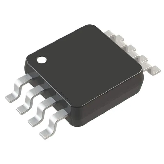
The LTC2055IMS8#PBF comes in an 8-lead MSOP package (3.00 mm × 3.00 mm body, 0.65 mm pitch). The supplier device package is 8-MSOP, which matches the 8-TSSOP footprint per JEDEC MO-187. The tube packaging means the parts ship in anti-static tubes — not tape-and-reel — so plan for manual placement or tube-fed pick-and-place if your line supports it.