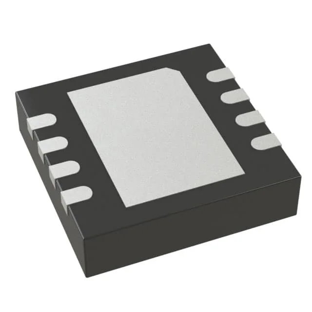
60 MHz dual op-amp in a 3x3 DFN — signal-chain fit
It delivers rail-to-rail output swing across a supply span from 3 V to 12.6 V, drawing 1.05 mA per channel.
75 µV offset and 55 mA output — DC precision and drive
The 1.5 µA input bias current is bipolar-typical and matters when the source impedance exceeds a few kilohms — plan for a bias-current error term in the noise gain calculation.
8-DFN footprint — thermal and layout notes
The pad is electrically connected to the negative supply (V−) on this device, so the PCB copper pour must be at the same potential. Solder-paste coverage on the pad should be about 50% stencil aperture to avoid floating the part during reflow.