Multi-topology regulator with a 2A switch — the fit check
The LT3580IMS8E#TRPBF is a current-mode step-up/step-up/step-down switching regulator IC from Analog Devices that operates in boost, Cuk, or SEPIC topology. The 2A internal switch sets the output power ceiling — in boost mode at 12V input, that switch current delivers roughly 24W output before hitting the current limit, but in SEPIC mode the same switch current must support both input and output, so the usable output power drops. Start from the reference design on page 18 of the datasheet to confirm the inductor saturation current against your load. The switching frequency range of 200kHz to 2MHz lets you trade inductor size against efficiency. At 2MHz the inductor footprint shrinks to a 4.7µH or 10µH chip, but switching losses in the 2A switch rise — expect 85–88% efficiency at full load. At 200kHz you gain a couple of points but need a 22µH or 33µH through-hole or larger shielded inductor. The frequency is set with a single resistor to ground; the RT pin is on page 7 of the datasheet.
Input and output voltage range — what the 42V switch rating means
The input range spans 2.5V to 32V, covering single-cell Li-ion up through 24V industrial rails. The switch is rated for 42V maximum — this is the absolute-maximum voltage the internal NPN switch can block when off. In a boost converter the output voltage can go to 42V, but the nominal output must stay below that ceiling with margin. For a 36V output rail, the 42V switch rating gives 6V headroom — comfortable for most loads, but a 40V output leaves only 2V margin and any transient overshoot during startup or load release risks avalanche stress on the switch. The output can be configured positive or negative — the Cuk and SEPIC topologies inherently produce an inverted output, so a single LT3580 can generate a -12V rail from a +5V input without a separate inverting charge pump. The adjustable output is set with a resistor divider from the FB pin; the internal reference is 1.215V typical, page 7 of the datasheet.
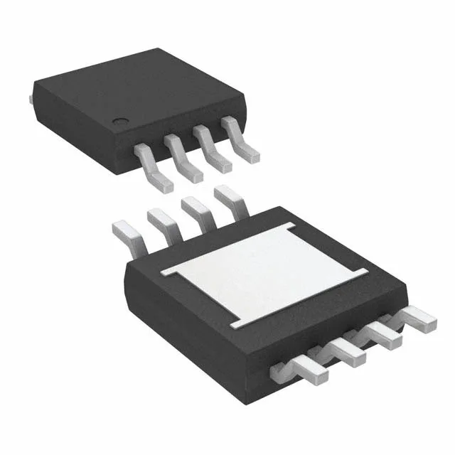
Package thermal reality — the exposed pad is not optional
At 2A switch current and 200kHz, the junction-to-ambient thermal resistance is roughly 40°C/W with a 1-square-inch copper pad — without that pad, the thermal resistance doubles and the junction temperature rises above the 125°C absolute maximum at moderate ambient. The datasheet layout example on page 16 shows the via pattern under the pad. This is the full industrial/automotive ambient band — the part can sit in an engine bay or outdoor enclosure as long as the PCB copper area keeps the junction below 125°C at full load. At 85°C ambient and 2A output, the junction will be around 105–115°C depending on the copper pour; that is inside the limit but leaves no margin for a hot spot.