200 mA LDO with 117 dB PSRR — the noise floor for precision analog rails
The LT3042IDD#PBF is an adjustable positive LDO regulator from Analog Devices, delivering up to 200 mA with a maximum input voltage of 20 V. Its headline feature is a PSRR that starts at 117 dB at 120 Hz and rolls off to 56 dB at 10 MHz — this means it rejects power-supply ripple and switching noise across the audio band into the low-MHz range, making it a fit for powering VCOs, ADC reference buffers, and sensitive analog front-ends where a clean rail directly determines signal-to-noise ratio. The adjustable output range from 0 V to 15 V lets it serve both low-voltage digital cores and higher-voltage analog supplies from a single regulator type, though the 200 mA ceiling limits it to lower-current branches of the power tree.
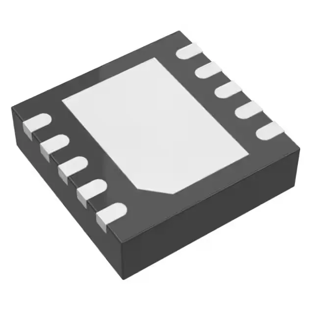
Maximum dropout voltage is 0.35 V at 200 mA load (typical). Built-in over-temperature and reverse-polarity protection reduce the need for external clamping diodes on the input, saving board space in dense layouts. The current-limit, enable, and power-good control features allow sequencing — the enable pin can be driven by a supervisor IC to hold the output off until the upstream rail is stable, and the power-good flag signals the downstream load that the output is within regulation. The 10-DFN (3x3 mm) package with exposed pad requires a thermal via array under the pad to conduct heat into the PCB ground plane. For a 200 mA load at 5 V input and 3.3 V output, the power dissipation is 0.34 W — the θJA for this package with proper board layout is typically around 50°C/W, so the junction stays well below the 125°C absolute maximum even at 85°C ambient, but a layout without thermal vias will push the junction temperature above the derating curve.
Active lifecycle and compliance — no end-of-life pressure
The junction temperature must not exceed 125°C even during fault conditions — the thermal protection circuit shuts down the regulator at approximately 165°C, but repeated cycling near that threshold degrades reliability.