Charge pump with bipolar output flexibility
The LT1054LCS8#PBF is a charge pump IC from Analog Devices that delivers up to 120 mA from a 3.5 V to 7 V input rail, with the output configurable as either positive or negative relative to the input. That bipolar output capability is what distinguishes it from a simple step-up boost — it generates a regulated negative rail from a positive supply, or doubles the input positive voltage, using only external capacitors and no inductor. Switching at 25 kHz, the part is optimised for low-noise analogue rails rather than high-frequency compactness — the lower switching frequency means larger external flying and reservoir capacitors (typically 10 µF to 100 µF electrolytic), but also keeps switching ripple well below the 100 kHz band where many op-amp PSRR curves roll off.
Package and board-fit constraints
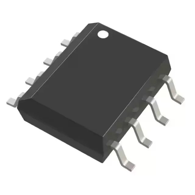
The supplier device package is 8-SO, which is the same mechanical outline as the industry-standard SO-8 — no footprint surprise when dropping it into a layout originally specified for a different charge pump. Delivered in tube packaging, this suits low-volume prototype and repair work where reel-fed pick-and-place is not the primary assembly method. For higher-volume builds, confirm the tube-to-reel transfer with your assembly house — the part is also available in tape-and-reel under a different order suffix.
Rated for 0°C to 100°C junction temperature, this is a commercial/industrial-grade part — not qualified for the -40°C automotive or military temperature extremes. It fits indoor equipment, bench instruments, telecom line cards, and industrial control boards where the ambient stays above freezing and below 85°C.