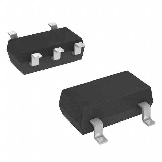
Analog Devices ADR01AKSZ-REEL7 — Analog & Data Acquisition

Analog Devices ADR01AKSZ-REEL7 Voltage Reference, 10 V ±0.1%

MPNADR01AKSZ-REEL7
End of Life

Analog Devices ADR01AKSZ-REEL7 series voltage reference, fixed 10 V output, ±0.1% tolerance, 20 µVp-p noise (0.1 Hz to 10 Hz), 25 ppm/°C drift, 10 mA output, SC-70-5, -40°C to 125°C.

$4.19Ref. price · indicative, final on quote
Packaging5-TSSOP, SC-70-5, SOT-353
RoHSROHS3 Compliant
Independent supplier — new & surplus stockAuthenticity-screened · ESD-safe packingListing updated Aug 2026

Specifications

ADR01AKSZ-REEL7 specifications
ParameterValue
Output typeFixed
MountingSurface Mount
Reference typeSeries
Voltage - input12V ~ 36V
Voltage - output (Min (Fixed))10V
Output current10 mA
Current - supply1mA
Operating temperature-40°C ~ 125°C (TA)
PackageTape & Reel (TR); Cut Tape (CT)
Tolerance±0.1%
Case5-TSSOP, SC-70-5, SOT-353
Noise - 0.1Hz to 10Hz20µVp-p
Temperature coefficient25ppm/°C

Product details

The ±0.1% tolerance at 25 °C sets the accuracy floor; the 25 ppm/°C temperature coefficient dominates drift over the -40°C to 125°C range. Output current is rated at 10 mA, which is enough to bias a single ADC reference input or a handful of op-amp stages, but not enough to power a multi-channel simultaneous-sampling array without buffering. The 1 mA supply current is the quiescent draw from the input rail (12 V to 36 V) — plan for that in your power budget, especially in loop-powered or battery-backed designs.

Housed in a 5-lead SC-70-5 (SOT-353), this is a compact surface-mount package for dense PCB layouts. Verify your land pattern against the supplier device package drawing.

For dual-sourcing resilience, the ADR01BKSZ-REEL7 is a pin-compatible sibling with tighter ±0.05% tolerance and a lower 9 ppm/°C drift — worth qualifying if your BOM needs a precision upgrade path without a board spin.

Frequently asked questions

What is the equivalent or replacement for ADR01AKSZ-REEL7?

The ADR01BKSZ-REEL7 is a pin-compatible sibling with the same 10 V output and SC-70-5 package but offers tighter ±0.05% tolerance and a lower 9 ppm/°C temperature coefficient. It's a drop-in upgrade for designs needing better drift performance without a PCB change.

What does the 20 µVp-p noise spec mean for my ADC design?

The 20 µVp-p noise over 0.1 Hz to 10 Hz is the low-frequency flicker noise that sits in the ADC's passband. For a 16-bit ADC with a 10 V reference, 1 LSB is about 153 µV — this reference's noise is roughly 13% of 1 LSB, so it won't dominate the noise floor in most precision acquisition chains.