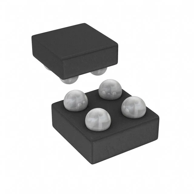
High-side load switch for low-voltage power rails
The Analog Devices ADP194ACBZ-R7 is a single-channel, high-side P-channel load switch designed for general-purpose power-domain switching. The switch delivers up to 500 mA continuous output current with a typical on-resistance of 55 mOhm, keeping conduction losses low in tight thermal budgets. A built-in slew-rate controlled turn-on limits inrush current and supply droop when the switch engages, which matters for sequencing sensitive loads like RF transceivers, sensor modules, or memory rails.
Package and assembly — WLCSP footprint
The ADP194ACBZ-R7 is supplied in a 4-ball WLCSP (0.74x0.74 mm body), a wafer-level chip-scale package with no molded encapsulant. A Cut Tape option is also available for prototype or low-volume builds.
Protection features — reverse current blocking
This switch includes reverse current protection, which prevents current from flowing backward from the output to the input when the switch is off. That is a practical safeguard in multi-rail designs where one rail may hold residual charge or where a battery is connected to the output side. The switch is controlled by a simple On/Off logic input (non-inverting), and no external Vcc supply is required — the gate drive is derived from the input voltage.
The wide temperature range also provides margin for self-heating at the 500 mA maximum load: with 55 mOhm Rds(on), I²R dissipation at full current is about 14 mW, which is negligible for the WLCSP package's thermal path through the PCB pads.
It is not subject to a last-time-buy or phase-out notice. For dual-sourcing or supply resilience, the ADP199ACBZ-R7 is a close functional peer — it shares the same package, pinout, and 500 mA output rating, but offers a lower 40 mOhm Rds(on) and a slightly lower minimum load voltage of 0.9 V. The ADP191ACBZ-R7 adds a load-discharge feature and also covers -40°C to 125°C, but its Rds(on) is higher at 80 mOhm.