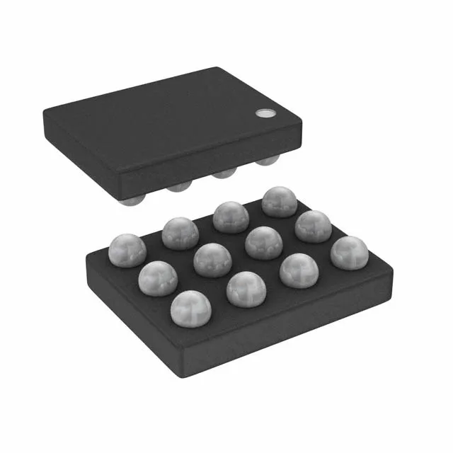
Analog Devices ADP1649ACBZ-R7 — Analog & Data Acquisition

ADP1649ACBZ-R7 Analog Devices LED Driver, Boost, 1A Flash

MPNADP1649ACBZ-R7
End of Life

Analog Devices ADP1649ACBZ-R7, DC DC Regulator LED Driver, Step-Up (Boost) topology, 1A Flash output, I²C dimming, 12-WLCSP package.

$2.66Ref. price · indicative, final on quote
Packaging12-WFBGA, WLCSP
RoHSROHS3 Compliant
Sourced new & surplus through independent channelsAuthenticity-screened · ESD-safe packingListing updated Aug 2026

Specifications

ADP1649ACBZ-R7 specifications
ParameterValue
TypeDC DC Regulator
MountingSurface Mount
Voltage - output4.575V ~ 5.425V
Voltage2.7V
Current - output (Channel)1A (Flash)
Frequency1.5MHz, 3MHz
I/O channels1
Operating temperature-40°C ~ 85°C (TA)
DimmingI²C
PackageTape & Reel (TR); Cut Tape (CT)
TopologyStep-Up (Boost)
ApplicationsCamera Flash
Case12-WFBGA, WLCSP
Internal switchYes

Product details

1 A flash boost driver with I²C control

The ADP1649ACBZ-R7 is a boost-mode DC-DC regulator designed specifically for camera flash LED applications, delivering up to 1 A of pulsed current to a single LED string. Output voltage is regulated between 4.575 V and 5.425 V, matching the forward voltage of a series flash LED while the internal switch handles the boost conversion. Dimming and control are managed over an I²C interface, which means the host processor sets the flash current level and timing directly — no external PWM pin needed.

Switching frequency and inductor choice

The part operates at either 1.5 MHz or 3 MHz switching frequency — the higher rate shrinks the inductor footprint but increases switching losses, so the choice balances PCB area against efficiency in the flash burst.

Package and board-fit for handheld designs

Housed in a 12-bump WLCSP measuring 1.5 x 2.0 mm (12-WLCSP), the ADP1649ACBZ-R7 is a true chip-scale package — the die is essentially the package, keeping the footprint minimal for space-constrained camera modules or wearable PCBs. Surface-mount assembly with standard lead-free reflow profiles applies; the WLCSP bumps are the only interface, so the PCB land pattern must match the 12-ball layout exactly.

It is suitable for both new designs and production sustainment. ROHS3 compliant, with no halogen or lead restrictions beyond the standard EU directive.

Frequently asked questions

What is the closest functional alternative to ADP1649ACBZ-R7?

The ADP1650ACBZ-R7 is a near pin-compatible peer in the same WLCSP package and I²C interface, but delivers 1.5 A flash output versus the ADP1649's 1 A.

Will ADP1649ACBZ-R7 drop into a board designed for ADP1650ACBZ-R7?

Both parts share the same 12-WLCSP package and I²C interface, so the PCB footprint is identical. The primary difference is the output current capability — 1 A vs 1.5 A — so the board's inductor and capacitor sizing should be checked if the full 1.5 A was required. For a 1 A flash load, it is a direct swap.