Analog Devices ADCLK905BCPZ-R7 — Clock & Timing ICs

ADCLK905BCPZ-R7 Analog Devices 7.5 GHz Clock Buffer SiGe

MPNADCLK905BCPZ-R7
End of Life

Analog Devices SiGe series, ADCLK905BCPZ-R7, Clock Buffer/Driver, Data, 1:1 fanout, 7.5 GHz max, ECL/NECL/PECL outputs, 16-LFCSP (3x3 mm), -40°C to 125°C, 2.375V to 3.63V supply.

$12.6Ref. price · indicative, final on quote
Packaging16-VFQFN Exposed Pad, CSP
StockContact for availability
MOQ1 pcs
  • 100% new & originalTraceable channels only — no refurbs, no pulls, no remarked parts.
  • Date & lot codes on quoteStated per line before you commit; label photos on request.
  • MSL-compliant ESD packingMoisture-sealed bags with indicator cards; reels photo-verified.
  • PayPal buyer protectionPay by T/T, PayPal or Payoneer — card payments covered end to end.

Specifications

ADCLK905BCPZ-R7 Technical Specifications
ParameterValue
TypeBuffer/Driver, Data
SeriesSiGe
Mounting typeSurface Mount
Voltage2.375V ~ 3.63V
Frequency7.5 GHz
Operating temperature-40°C ~ 125°C
InputClock
OutputECL, NECL, PECL
PackageTape & Reel (TR); Cut Tape (CT)
Case16-VFQFN Exposed Pad, CSP
Number of circuits1
Ratio - Input:Output1:1
Differential - Input:OutputYes/Yes

Product details

7.5 GHz buffer for clock distribution

The ADCLK905BCPZ-R7 is a single-channel clock buffer from Analog Devices' SiGe series, rated for a maximum frequency of 7.5 GHz. That bandwidth covers the fastest serial data converters, FPGA reference clocks, and RF sampling ADCs — the part doesn't limit the clock tree before the signal reaches the load. It accepts a differential clock input and delivers a differential output in ECL, NECL, or PECL logic levels, selectable via the supply voltage. The 1:1 fanout keeps the signal path simple — one clean copy of the input, no added skew from a splitter.

Supply and temperature range

The part operates from a single 2.375V to 3.63V supply, so it can run directly off a 2.5V or 3.3V rail without an extra LDO.

Package and layout notes

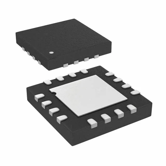
Housed in a 16-lead LFCSP with exposed pad measuring 3x3 mm. The exposed paddle must be soldered to a ground plane for thermal and electrical performance — at 7.5 GHz, a floating paddle adds inductance that degrades signal integrity.

Frequently asked questions

What is the difference between ADCLK905BCPZ-R7 and ADCLK925BCPZ-R7?

Both are SiGe clock buffers with the same 7.5 GHz bandwidth and output logic family. The ADCLK905 provides a 1:1 fanout (one input to one output), while the ADCLK925 offers a 1:2 fanout (one input to two outputs). If your design needs to drive multiple loads from a single clock source, the ADCLK925 saves an extra buffer stage.

Is ADCLK905BCPZ-R7 compatible with 3.3V logic?

Yes. The supply range of 2.375V to 3.63V covers both 2.5V and 3.3V rails. When powered at 3.3V, the output swings PECL levels that are directly compatible with 3.3V CML or LVPECL inputs on downstream devices. No level translator is needed.