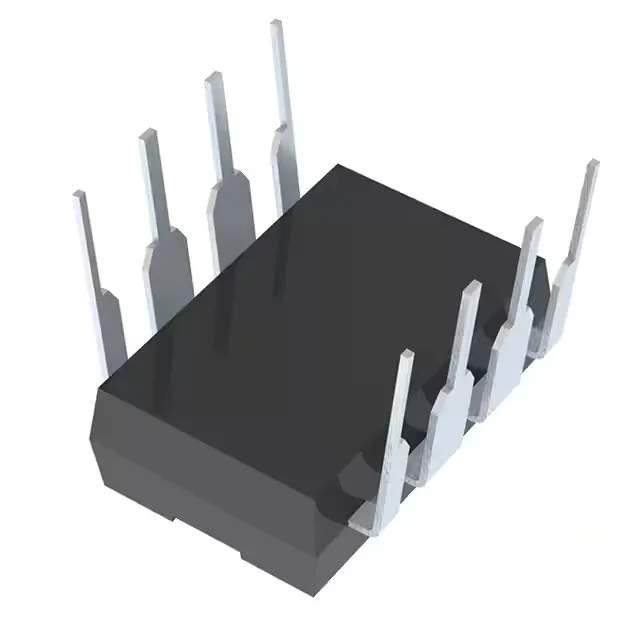
Package and integration story
The AD648KNZ comes in an 8-DIP (0.300", 7.62mm) through-hole package, supplier device package 8-PDIP. This footprint mates with standard 0.100-inch pitch DIP sockets or can be soldered directly into plated through-holes on a two-layer board — no fine-pitch routing needed. The tube packaging keeps the leads aligned during storage and kitting.
What the key ratings mean for the BOM
The J-FET input stage delivers 3 pA typical input bias current — this matters for high-impedance sensor front-ends where a bipolar input's base current would drop voltage across the source resistance and shift the DC operating point. The 300 µV input offset voltage is the DC error the system sees at the output; for a gain of 100, that is 30 mV at the output before any signal. Slew rate is 1.8V/µs, which sets the maximum rate of change at the output. For a 10 V peak-to-peak output swing, the full-power bandwidth is about 28 kHz — above that the output distorts into a triangle wave. The 1 MHz gain-bandwidth product and -3dB bandwidth mean the open-loop gain drops to unity at 1 MHz; closed-loop gain of 10 gives a 100 kHz signal bandwidth. Supply current is 340 µA per channel, totalling 680 µA for both amplifiers. This is a low quiescent draw for a dual op-amp, suitable for battery-powered or loop-powered signal conditioning where every microamp counts. The supply span from 9 V to 36 V covers single-supply (9 V, 12 V, 24 V) and split-supply (±4.5 V to ±18 V) rails without needing a separate regulator. Output drive is 15 mA per channel — enough to drive a 2 kΩ load to ±15 V swing or feed the input of an ADC with a sample-and-hold capacitor. The 0°C to 70°C commercial temperature range fits controlled indoor environments, instrumentation, and bench equipment.