Programmable gain for analog front-ends
The AD526JNZ is a single-channel programmable gain amplifier (PGA) from Analog Devices, built for analog signal-conditioning chains where the gain needs to change under digital control — think data-acquisition front-ends, multiplexed sensor inputs, or test equipment that handles multiple input ranges without swapping resistors. With a 24 V/µs slew rate and 4 MHz -3 dB bandwidth, this PGA handles moderate-speed signals up to a few hundred kilohertz without slew-rate limiting; the 10 mA supply current is typical for a precision PGA in this class.
Supply range and signal-chain accuracy
The 9 V to 33 V supply span means it runs off common ±5 V to ±15 V analog rails — the same rails that power the ADC and reference in a typical DAQ board. Input bias current is 50 pA typical, and input offset voltage is 400 µV — both matter when the front-end interfaces with a high-impedance sensor like a pH probe or a photodiode amplifier, where bias current flowing through the source resistance creates an offset error. Output current is rated 10 mA per channel, enough to drive the input of a successive-approximation ADC's sample-and-hold capacitor through a small series resistor, but not enough to drive a cable or a heavy load directly.
Through-hole DIP-16 — board integration
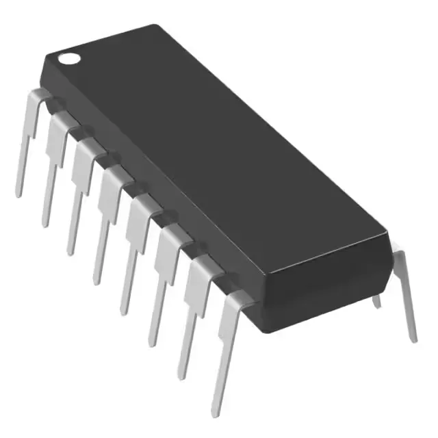
Housed in a 16-pin DIP (0.300" body width, 7.62 mm row spacing) with through-hole mounting, the AD526JNZ is a natural fit for prototyping boards, breadboards, or legacy designs that avoid surface-mount assembly — the 16-PDIP supplier package matches standard 0.100" pitch sockets. The commercial temperature grade (0°C to 70°C) limits deployment to indoor, temperature-controlled environments — not suitable for industrial enclosures or outdoor gear without active thermal management.
Active lifecycle and compliance
ROHS3 compliant, and supplied in a tube — the standard DIP-16 shipping format.