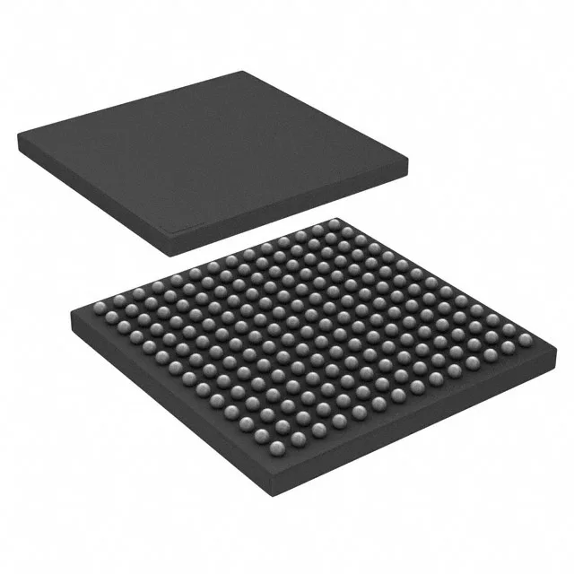
23360 logic cells, 100 I/O — resource budget for the design
The AMD XC7S25-1FTGB196I is a Spartan®-7 FPGA with 23360 logic elements (cells) organised into 1825 CLB slices, giving you a clear resource ceiling for combinatorial and registered logic before you start the place-and-route iteration. The 100 user I/O are bonded out on the 196-ball CSBGA package — that is 96 fewer balls than the package's full matrix, so the outer rows are mostly Vccio and GND. The 1658880 total block RAM bits (about 2 Mbit) handle moderate FIFO or line-buffer depth without going to external SRAM.
Industrial temp grade and 0.95–1.05 V core rail
The core supply must stay within 0.95 V to 1.05 V — a 50 mV window. That means a 1.0 V nominal rail with ±2.5% regulation, which a standard 1.0 V LDO or POL converter holds easily, but the PCB IR drop from the regulator to the BGA balls eats into that budget. Four-layer board with a dedicated power plane is the practical floor.
196-CSBGA footprint — layout and rework reality
The 196-ball CSBGA measures 15 mm × 15 mm with a 0.80 mm ball pitch — tight enough that a single via-in-pad per ball is the norm, but not so fine that you need microvias or HDI stack-up. The outer two rows fan out on a 4-layer board with 0.20 mm trace/space. A rework profile with a top-side preheat at 150°C and a peak at 245°C handles the joint without lifting the adjacent passives.
The Spartan-7 family is AMD's cost-optimised 28 nm node, positioned below the Artix-7 in density and above the older Spartan-6 in performance-per-watt. No pin-compatible second source exists; the BOM carries a single-source risk that a volume RFQ should hedge.