Logic density and memory — 23360 LEs with 1.6 Mbit block RAM
The XC7S25-1CSGA225I packs 23360 logic elements (cells) into 1825 CLB slices — enough for moderate glue logic, a soft-core MCU, or a custom DSP datapath without spilling into a larger device. The 1658880 total RAM bits (1.6 Mbit) distributed as block RAM handle FIFOs, line buffers, and small lookup tables on-chip, keeping external SRAM off the BOM for many control-plane applications. With 150 user I/O accessible on the 225-ball CSGA package, the device can interface to a parallel ADC/DAC bank, a DDR memory bus, or multiple SPI/I2C peripherals simultaneously. The 0.95 V to 1.05 V core supply means the FPGA sits on a single 1.0 V rail — the same rail that powers the adjacent SoC or processor, simplifying the power-tree design.
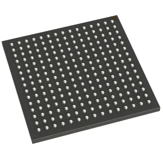
Package and board integration — 225-ball CSGA, 13x13 mm
The 225-LFBGA / CSPBGA package (supplier device package 225-CSGA) measures 13x13 mm with a 0.80 mm ball pitch — a standard fine-pitch BGA that routes on a 4-layer PCB without microvias. The surface-mount footprint matches the XC7S50 and XC7S100 siblings in the same package, so a single board layout can span multiple density grades by swapping the BOM line. The device is ROHS3 compliant, so it ships lead-free and meets the EU RoHS directive for equipment placed on the market after 2015.