Logic fabric and memory headroom for the BOM
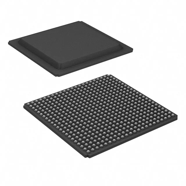
The XC7A35T-1FGG484C packs 33280 logic elements across 2600 configurable logic blocks, with 1843200 total RAM bits on-chip. For a typical glue-logic or sensor-fusion design, that block RAM covers small frame buffers, FIFOs, and coefficient tables without reaching for external SRAM — the 1.8 Mbit ceiling is the line between a single-chip FPGA solution and one that needs a companion memory chip on the board. The 250 user I/O on the 484-BBGA package (, 23x23 mm) gives enough pins to connect a parallel ADC bus, a DDR memory interface, and a few dozen general-purpose signals before the bank count becomes the constraint. The 0.95 V to 1.05 V core supply is standard for the 28 nm process node — any switching regulator on the board that delivers 1.0 V at 1 A will bias this device correctly.
Temperature grade and board integration
The commercial temperature range (0°C to 85°C junction,) restricts this variant to controlled indoor environments — server rooms, test equipment, industrial cabinets with active cooling. For an outdoor telecom or automotive deployment, the industrial-grade (-40°C to 100°C) sibling would be the correct pick, but the 484-BBGA package and pinout are identical, so the PCB layout transfers directly. The 484-ball BGA with 23x23 mm body requires a 4-layer board minimum for fan-out — the inner rows need microvias or blind vias to escape to the inner layers. Decoupling capacitor placement under the BGA is not possible with this pitch; plan for a ring of 0402 or 0201 caps on the top side within 5 mm of the package edge, one per power ball pair.