Logic capacity and I/O budget for the BOM
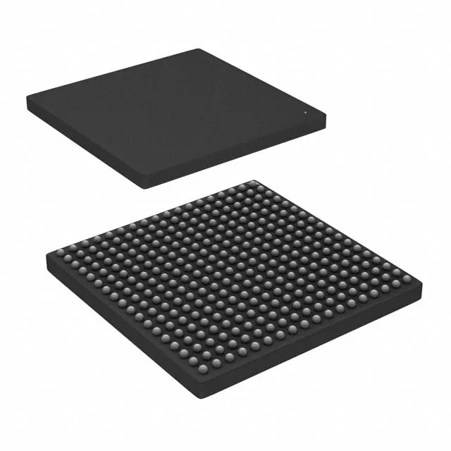
The XC7A25T-2CSG325I is an AMD Artix-7 FPGA with 23,360 logic cells distributed across 1,825 CLB slices. Each slice contains four 6-input LUTs and eight flip-flops, giving the synthesis tool enough fabric for a 32-bit RISC-V soft core plus peripheral glue logic, or a moderate image-processing pipeline. 150 user I/O are brought out to a 324-ball CSPBGA package with a 15x15 mm body. The 0.8 mm ball pitch requires a four-layer PCB for full fan-out; a two-layer board can route only the outer two ball rows. The I/O banks operate at 1.2V to 3.3V, matching common memory and sensor interfaces without external level translation.
On-chip memory and supply rail tolerance
Total block RAM is 1,658,880 bits, organized as 90 blocks of 18 Kbit each. This is sufficient for a 1280x720 line buffer at 8-bit depth, or a 256-entry 64-bit FIFO for clock-domain crossing. The core supply voltage range is 0.95V to 1.05V; the nominal 1.0V rail must be regulated within ±50 mV to meet the -2 speed-grade timing across temperature. Operating temperature spans -40°C to 100°C, which qualifies the device for industrial environments such as outdoor base stations, motor drives, and engine-bay controllers. The industrial grade also means the device is screened to tighter limits than the commercial variant, reducing the risk of timing failures at temperature extremes.
Active lifecycle and compliance posture
It is suitable for both new designs and volume production. ROHS3 compliant, with no RoHS exemption expiry concerns for EU-market builds.