Logic density and I/O budget for the BOM
The XC7A35T-2FTG256I packs 33,280 logic elements across 2,600 CLB slices — enough gate budget for a moderate-throughput interface controller or sensor fusion pipeline without spilling into a larger die. 170 user I/O in a 256-ball BGA means roughly two-thirds of the balls are signal pins; the rest are power and ground, which keeps the simultaneous-switching-noise margin healthy on a four-layer board. On-chip block RAM totals 1,843,200 bits — about 225 KB — enough for a small frame buffer or a coefficient lookup table without hitting external memory latency.
Package, supply, and temperature grade
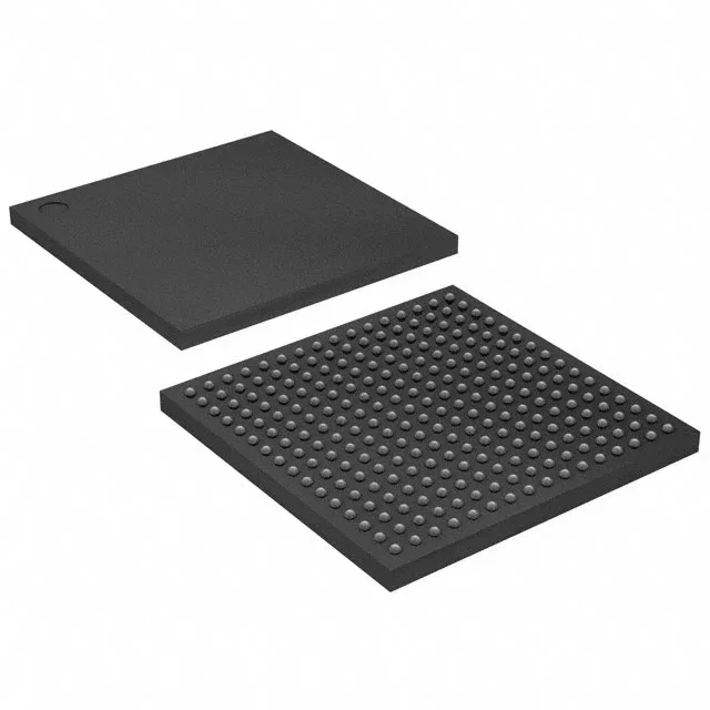
The 256-FTBGA (17x17 mm) footprint is a 1.0 mm ball-pitch array — routable on four layers without microvias, though the inner rows need dog-bone fan-out to escape the BGA field. Core voltage is 0.95 V to 1.05 V; the 100 mV tolerance means the on-board regulator must hold within ±50 mV under load transients, or the FPGA may fail to configure at cold start.
Lifecycle and sourcing posture
ROHS3 compliant — no exemption-listed substances; the component ships in tray packaging, which is the standard medium for BGA devices that must stay flat during transit.