Logic fabric and memory headroom
The XC7A15T-3FTG256E packs 16,640 logic cells arranged in 1,300 CLBs, with 921,600 bits of block RAM distributed across the fabric. That RAM budget covers moderate FIFO depth, small frame buffers, or coefficient storage without gluing external SRAM onto the board. The 170 user I/O are banked and support multiple voltage standards within the 0.95 V to 1.05 V core supply envelope.
Package and board-fit realities
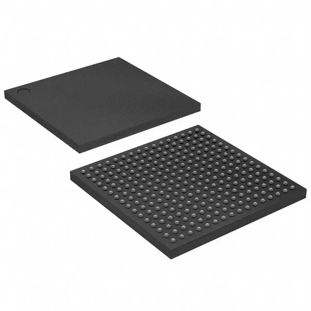
Housed in a 256-ball FTBGA (17 mm × 17 mm), the 0.80 mm ball pitch is routable on a standard 4-layer PCB with via-in-pad avoided by dog-boning to the inner rows. The exposed thermal pad on the bottom of the package requires a solid copper plane and at least 9 thermal vias to keep the junction below 100 °C under full utilization. The core voltage rail (0.95 V–1.05 V) must be within ±50 mV at the ball — a remote-sense regulator or tight-layout local LDO is recommended. The 1.0 V nominal draws the bulk of the device current; the PCB stack-up should dedicate an inner layer to this plane.
Active lifecycle and compliance posture
The tray packaging (MSL 3 typical for FTBGA) means the floor life is 168 hours once the seal is broken; a bake is required if the exposure window is exceeded.