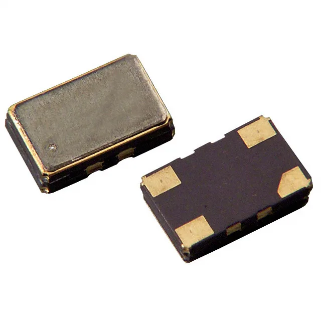
Why 19.2 MHz VCTCXO fits timing-critical RF
The ASVTX-11-A-19.200MHZ-T is a voltage-controlled temperature-compensated crystal oscillator (VCTCXO) operating at 19.2 MHz with a clipped sine wave output. The clipped sine wave is the standard reference format for cellular and GNSS modules — it delivers cleaner spectral characteristics than a square wave while maintaining enough amplitude to drive the RFIC reference input directly, without additional buffering. ±2.5ppm frequency stability across the full -30°C to 75°C operating window is what separates a VCTCXO from a plain TCXO. In GPS/GNSS timing and cellular base station references, that drift budget is the difference between a sub-meter position fix and losing lock when the enclosure heats up — the base station handover margin similarly depends on holding that reference across temperature.
Board integration and thermal profile
The exposed pad on the underside carries the ground reference; the pad geometry and stencil opening at the package perimeter govern solder joint reliability more than the centre pads themselves, especially in thermal cycling. The device draws up to 1.5 mA from the 3 V supply — higher than a passive crystal because the internal compensation loop needs power. Budget this into the supply rail and decoupling design; the oscillator load current is constant, not pulsed, so a 100 nF local bypass is typically sufficient to clean supply noise from adjacent switching rails.
BOM placement and sourcing posture
The ASVTX-11 series spans multiple frequencies, but substituting a different frequency grade requires confirming the target PLL ratio and loop bandwidth on the baseband chip before committing — the RFIC datasheet will specify the exact reference tolerance budget, not just the raw ±2.5ppm figure.