Why ±1.5ppm is the spec that matters here
The ASVTX-13-A-38.400MHZ-D15-T is a VCTCXO — voltage-controlled temperature-compensated crystal oscillator — delivering 38.4 MHz in clipped sine wave output. The headline rating is ±1.5ppm frequency stability across the full operating range of -30°C to 85°C, which means the total timing error budget over temperature stays within 1.5 parts per million — critical for any PLL reference or ADC clock where phase noise integrates directly into the signal chain.
Clock tree integration — supply, current, and the 3V rail
Powered from a single 3V rail drawing up to 2mA — the supply current is low enough that a dedicated LDO is often unnecessary if the upstream rail is clean, but a noisy digital rail will couple through the VCTCXO's control voltage sensitivity. The clipped sine wave output presents a lower harmonic content than a CMOS square wave, reducing spurious content in the downstream mixer or PLL — the phase-noise plot does not lie, and a clean output stage means less cleanup work in the loop filter.
2.00×1.60mm footprint — what the 4-SMD no-lead package means on the board
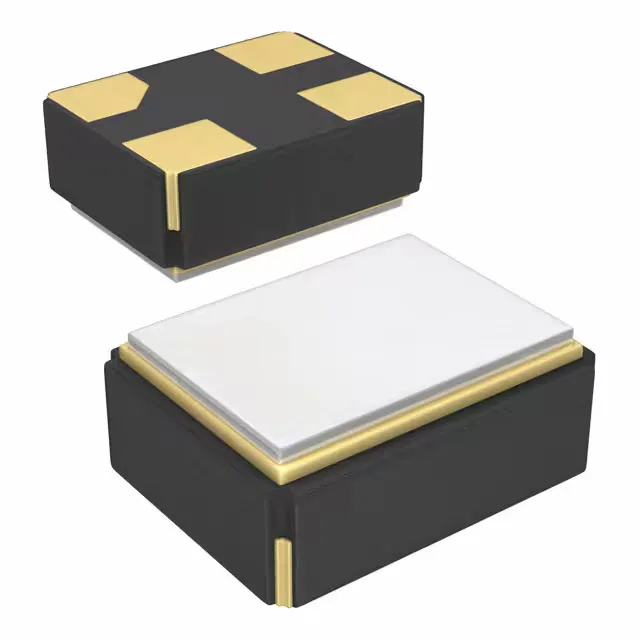
The 2.00 mm × 1.60 mm body with 0.80 mm seated height is the standard compact oscillator footprint — the no-lead (DFN-style) terminations sit flush to the PCB, so the land pattern must be accurate or the coplanarity error shifts the resonance. Solder paste volume and reflow profile matter more than usual: undersized pads increase standoff tilt; oversized pads can shift the effective capacitance loading the crystal resonator and detune the trim range. The 3V supply decoupling should be as close to the device as the layout allows — typically 100 nF plus optional 10 nF for the HF content.