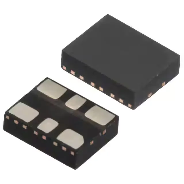
Supply and power-gating characteristics
The ASEMPC-68.000MHZ-T3: The oscillator draws up to 35 mA from a 2.25–3.6 V rail when active, and the enable/disable pin lets the firmware or host MCU gate the output off — cutting the current to a maximum of 26 mA. For a battery-powered device this is a meaningful budget saving: the part idles at the disable level rather than running full current between clock edges, so a sensor node that sleeps between measurements extends its standby runtime. The 3.20mm × 2.50mm 6-SMD no-lead package sits in the same land pattern as a standard half-width XO — the PCB layout challenge is the supply decoupling: the oscillator draws pulsed current on every output edge, so a 100 nF bypass placed within 2 mm of the supply pin handles the transient; a second 10 nF extends the high-frequency attenuation further up the band.
Active lifecycle — sourcing and BOM posture
The part carries an Active product status from the manufacturer, with no stated NRND or EOL notice in the ledger. No official second-source or cross-reference sibling appears in the available record, so this is a single-source timing part in the ASEMP series — a BOM should carry a second-source requirement flagged at RFQ so a compatible alternative can be qualified before the design locks.