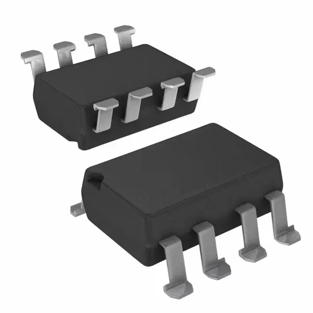
Vishay VO3120-X019T — Optoisolators

VO3120-X019T Vishay Optoisolator – 5300 Vrms

MPNVO3120-X019T
End of Life

Vishay VO3120-X019T, single-channel optical coupling gate driver, 5300 Vrms isolation, 2.5 A peak output, 8-SMD gull wing package, -40 to 110 °C

$2.42Ref. price · indicative, final on quote
Packaging8-SMD, Gull Wing
StockContact for availability
MOQ1 pcs
  • 100% new & originalTraceable channels only — no refurbs, no pulls, no remarked parts.
  • Date & lot codes on quoteStated per line before you commit; label photos on request.
  • MSL-compliant ESD packingMoisture-sealed bags with indicator cards; reels photo-verified.
  • PayPal buyer protectionPay by T/T, PayPal or Payoneer — card payments covered end to end.

Specifications

VO3120-X019T Technical Specifications
ParameterValue
Mounting typeSurface Mount
Voltage - isolation5300Vrms
Voltage - output supply15V ~ 32V
Voltage - forward (Vf)1.6V (Max)
Current - peak output2.5A
Current - output high, low2.5A, 2.5A
Current - DC forward (If)25 mA
Operating temperature-40°C ~ 110°C
Pulse width distortion200ns
Approval agencycUR, UR, VDE
PackageTape & Reel (TR); Cut Tape (CT)
TechnologyOptical Coupling
Case8-SMD, Gull Wing
Number of channels1
Rise (Fall time)100ns, 100ns
Propagation delay tpLH (tpHL)400ns, 400ns
Common mode transient immunity25kV/µs

Product details

Gate-drive optocoupler for IGBT and MOSFET switching

The VO3120-X019T is a single-channel optical coupling gate driver from Vishay, designed to drive IGBTs and power MOSFETs in motor drives, inverters, and industrial power supplies. It delivers a 2.5 A peak output current with 5300 Vrms isolation between the logic-side input and the power-stage output. The 25 kV/µs minimum common-mode transient immunity keeps the output state stable when the power stage switches at high dv/dt — a requirement for SiC and GaN inverter stages where fast edges couple noise across the isolation barrier.

Parametric limits that set the drive budget

The output supply range of 15 V to 32 V covers the typical gate-drive rails for IGBT modules (15 V on, -5 V to -8 V off) and standard MOSFET drivers. The 2.5 A source and sink current is symmetric, so turn-on and turn-off gate charge delivery are balanced — no need for a separate pull-down resistor on the gate. Propagation delay is 400 ns max for both tpLH and tpHL, with a pulse-width distortion ceiling of 200 ns. For a 20 kHz PWM carrier, that delay adds about 0.8 % dead-time error — the controller's dead-time insertion must account for this. Rise and fall times are 100 ns typical, which limits the gate-drive edge rate. For a 10 nC gate charge (typical of a 50 A IGBT module), the 2.5 A peak charges the gate in roughly 4 ns, but the 100 ns rise time is dominated by the optocoupler's internal output stage, not the external gate resistor.

Active production — no LTB watch needed

Approvals include cUR, UR, and VDE, which satisfy the safety-agency requirements for reinforced insulation in motor-drive and power-supply designs sold into North American and European markets.

Frequently asked questions

Is VO3120-X019T suitable for driving IGBTs or MOSFETs?

Yes. The 2.5 A peak output and 15 V to 32 V supply range are well matched to the gate-drive requirements of medium-power IGBT modules and power MOSFETs. The 25 kV/µs CMTI ensures reliable switching in inverter environments with fast voltage transients.

Does VO3120-X019T support UVLO (undervoltage lockout)?

The evidence does not list UVLO as a feature. The datasheet should be consulted for the detailed output-stage protection. The 15 V minimum supply suggests the part expects the user to ensure the supply rail is above the gate-threshold region.