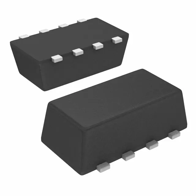
Vishay SI5908DC-T1-E3

SI5908DC-T1-E3 TrenchFET Dual N-Ch MOSFET, 20V 4.4A

MPNSI5908DC-T1-E3
End of Life

Vishay TrenchFET® SI5908DC-T1-, dual N-channel logic-level MOSFET, 20V Vdss, 4.4A continuous drain, 40mOhm Rds(on) at 4.5V, 7.5nC gate charge, 1206-8 ChipFET™ package, -55°C to 150°C.

$1.41Ref. price · indicative, final on quote
Packaging8-SMD, Flat Lead
StockContact for availability
MOQ1 pcs
  • 100% new & originalTraceable channels only — no refurbs, no pulls, no remarked parts.
  • Date & lot codes on quoteStated per line before you commit; label photos on request.
  • MSL-compliant ESD packingMoisture-sealed bags with indicator cards; reels photo-verified.
  • PayPal buyer protectionPay by T/T, PayPal or Payoneer — card payments covered end to end.

Specifications

SI5908DC-T1-E3 Technical Specifications
ParameterValue
SeriesTrenchFET®
FET type2 N-Channel (Dual)
Mounting typeSurface Mount
Drain to source voltage20V
Current - continuous drain (Id) @ 25°C4.4A
Power - max1.1W
Operating temperature-55°C ~ 150°C (TJ)
PackageTape & Reel (TR); Cut Tape (CT)
FET featureLogic Level Gate
Case8-SMD, Flat Lead
Vgs(th) (Max) @ id1V @ 250µA
Rds on (Max) @ id, vgs40mOhm @ 4.4A, 4.5V
Gate charge (Qg) (Max) @ vgs7.5nC @ 4.5V

Product details

Dual N-channel logic-level switch in a flat-lead package

The SI5908DC-T1-E3: The SI5908DC-T1-: The Vishay SI5908DC-T1- is a dual N-channel MOSFET from the TrenchFET series, built for low-voltage rail switching where a logic-level gate threshold is needed. Each channel is rated for 20 V drain-source and 4.4 A continuous drain current at 25 °C, with a maximum on-resistance of 40 mOhm at 4.5 V gate drive. The 1206-8 ChipFET package keeps the footprint small — the flat leads sit flush on the board, making it a fit for dense layouts where vertical clearance is tight. The dual-channel configuration saves board area compared to two single MOSFETs when you need independent load switching or a half-bridge leg.

Rds(on) and gate charge at logic-level drive

The 1 V max gate threshold at 250 µA means the part turns on cleanly from a 3.3 V logic signal — no separate gate-driver IC needed for moderate switching frequencies. Total gate charge is 7.5 nC at 4.5 V. That is low enough that a microcontroller GPIO can drive the gate directly at tens of kHz without excessive switching loss.

Temperature grade and deployment envelope

The junction temperature range spans -55 °C to 150 °C, which is the military-grade envelope. This part suits avionics, satellite payloads, and downhole instrumentation where the ambient can swing well beyond industrial limits. The 1.1 W maximum power dissipation in the ChipFET package is the thermal constraint — derate for high ambient or limited copper area on the PCB.

Frequently asked questions

Where can I buy SI5908DC-T1-E3?

Buyers need immediate sourcing options to place orders and avoid project delays.

What is the price of SI5908DC-T1-E3?

Pricing directly affects BOM cost calculations and comparison with alternatives.

Is SI5908DC-T1-E3 obsolete?

Lifecycle status determines long-term availability and risk of last-time buy decisions.

What is a replacement for SI5908DC-T1-E3?

Engineers and buyers need drop-in alternatives when the original is unavailable or EOL.

What are the specifications of SI5908DC-T1-E3?

Detailed specs verify fit for the application and avoid design errors.

What is the lead time for SI5908DC-T1-E3?

Lead time impacts production schedules and inventory planning for sourcing buyers.