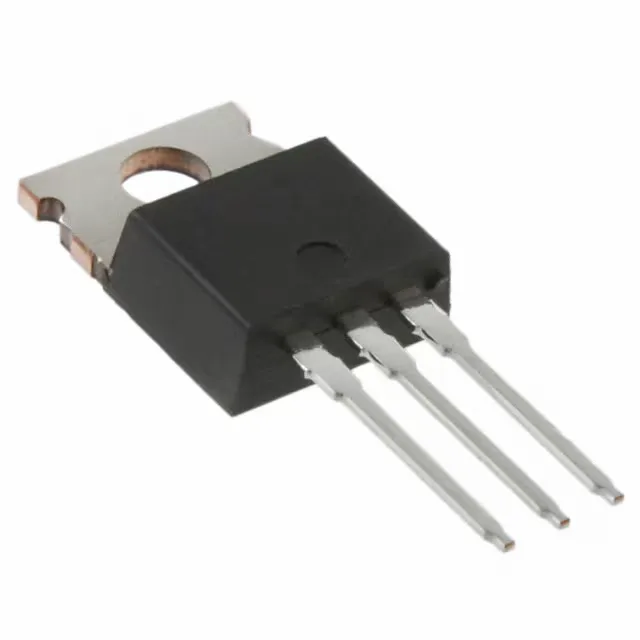
Vishay IRF840APBF

IRF840APBF N-Channel MOSFET, 500V 8A TO-220AB

MPNIRF840APBF
End of Life

Vishay IRF840APBF, N-Channel MOSFET, 500 V drain-source, 8 A continuous drain, 850 mOhm Rds(on) at 10 V, TO-220AB through-hole package, -55 to 150°C junction temperature.

$1.97Ref. price · indicative, final on quote
PackagingTO-220-3
StockContact for availability
MOQ1 pcs
  • 100% new & originalTraceable channels only — no refurbs, no pulls, no remarked parts.
  • Date & lot codes on quoteStated per line before you commit; label photos on request.
  • MSL-compliant ESD packingMoisture-sealed bags with indicator cards; reels photo-verified.
  • PayPal buyer protectionPay by T/T, PayPal or Payoneer — card payments covered end to end.

Specifications

IRF840APBF Technical Specifications
ParameterValue
FET typeN-Channel
Mounting typeThrough Hole
Drain to source voltage500 V
Drive voltage (Max rds on, min rds on)10V
Current - continuous drain (Id) @ 25°C8A (Tc)
Power dissipation125W (Tc)
Operating temperature-55°C ~ 150°C (TJ)
PackageTube
Vgs±30V
TechnologyMOSFET (Metal Oxide)
CaseTO-220-3
Vgs(th) (Max) @ id4V @ 250µA
Rds on (Max) @ id, vgs850mOhm @ 4.8A, 10V
Gate charge (Qg) (Max) @ vgs38 nC @ 10 V
Input capacitance (Ciss) (Max) @ vds1018 pF @ 25 V

Product details

500 V, 8 A N-channel — the TO-220 workhorse for offline power stages

The IRF840APBF is a Vishay N-channel power MOSFET in a TO-220AB through-hole package, rated for 500 V drain-source breakdown and 8 A continuous drain current at 25°C case temperature. It targets high-voltage switching applications such as flyback converters, offline AC-DC power supplies, and motor drive circuits where the 500 V blocking voltage provides margin for rectified 240 VAC rails. With a maximum on-resistance of 850 mOhm at 4.8 A and 10 V gate drive, conduction losses stay manageable for loads up to a few amps. The 38 nC total gate charge keeps the gate-drive power low at moderate switching frequencies — a practical fit for 50–100 kHz hard-switched topologies.

Gate drive and switching — what the numbers mean at the bench

The 10 V gate drive voltage is specified for both the maximum and minimum Rds(on) — this part expects a full 10 V gate signal to achieve the rated on-resistance. The gate threshold is 4 V maximum at 250 µA drain current, so a 5 V logic-level gate drive will not fully enhance the channel; plan for a dedicated gate driver or a bootstrap supply above 10 V. Input capacitance is 1018 pF typical at 25 V drain-source — a moderate figure that does not require a heroic gate-driver for switching frequencies under 100 kHz. The 38 nC gate charge translates to roughly 3.8 mA average gate-drive current at 100 kHz, well within the capability of a standard MOSFET driver like the TC4427.

Thermal handling and package rework

Maximum power dissipation is 125 W at the case, but the real thermal limit depends on the heatsink. The TO-220AB package has a metal tab that must be electrically isolated or connected to the drain node — the tab is the drain. For rework, the through-hole leads are easy to desolder with a solder sucker or wick; the tab can be soldered to a PCB pad or bolted to a heatsink with a TO-220 mounting kit.

Frequently asked questions

Is IRF840APBF RoHS compliant?

Yes, the IRF840APBF is ROHS3 compliant, meeting current EU and global environmental requirements for lead-free soldering processes.

What is the closest functional second-source for IRF840APBF?

The IRFP440PBF is a close functional peer — also a 500 V N-channel MOSFET in a through-hole package, with 8.8 A continuous drain current and similar 850 mOhm Rds(on). However, the IRFP440PBF has a ±20 V maximum gate-source rating (vs ±30 V on the IRF840APBF) and a higher 63 nC gate charge. Verify pin compatibility and thermal performance in your specific layout before substituting.