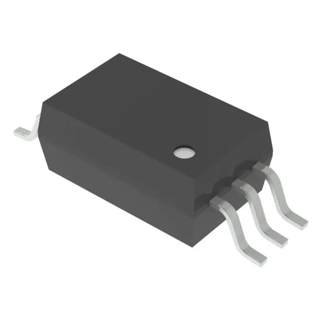
Toshiba Semiconductor TLP5754(D4-TP4,E — Optoisolators

TLP5754(D4-TP4,E Toshiba Optocoupler Gate Driver 4A 5000Vrms

MPNTLP5754(D4-TP4,E
End of Life

Toshiba Semiconductor TLP5754(D4-TP4,E, optical coupling gate-drive optocoupler, 1 channel, 4 A peak output, 5000 Vrms isolation, 6-SOIC package, Tape & Reel

$2.92Ref. price · indicative, final on quote
Packaging6-SOIC (0.295", 7.50mm Width)
StockContact for availability
MOQ1 pcs
  • 100% new & originalTraceable channels only — no refurbs, no pulls, no remarked parts.
  • Date & lot codes on quoteStated per line before you commit; label photos on request.
  • MSL-compliant ESD packingMoisture-sealed bags with indicator cards; reels photo-verified.
  • PayPal buyer protectionPay by T/T, PayPal or Payoneer — card payments covered end to end.

Specifications

TLP5754(D4-TP4,E Technical Specifications
ParameterValue
Mounting typeSurface Mount
Voltage - isolation5000Vrms
Voltage - output supply15V ~ 30V
Voltage - forward (Vf)1.55V
Current - peak output4A
Current - output high, low3A, 3A
Current - DC forward (If)20 mA
Operating temperature-40°C ~ 110°C
Pulse width distortion50ns
Approval agencyCQC, CSA, cUL, UL, VDE
PackageTape & Reel (TR); Cut Tape (CT)
TechnologyOptical Coupling
Case6-SOIC (0.295\", 7.50mm Width)
Number of channels1
Rise (Fall time)15ns, 8ns
Propagation delay tpLH (tpHL)150ns, 150ns
Common mode transient immunity35kV/µs

Product details

Gate-drive optocoupler for IGBT and MOSFET switching

The TLP5754(D4-TP4,E is a 1-channel optical coupling gate driver from Toshiba, delivering 4 A peak output current to directly drive IGBTs and power MOSFETs without an external buffer stage. It provides 5000 Vrms isolation between input and output, meeting reinforced insulation requirements for industrial motor drives, inverters, and switch-mode power supplies. Common-mode transient immunity is rated at 35 kV/µs minimum, which keeps the output state stable under the fast dv/dt edges present in half-bridge and three-phase inverter switching nodes.

Switching speed and drive strength for power-stage design

Typical rise and fall times are 15 ns and 8 ns respectively, with a maximum propagation delay of 150 ns in both directions — this timing symmetry simplifies dead-time calculation in complementary-switch topologies. Pulse width distortion is held to 50 ns max, so the on-time accuracy at the power switch is preserved even at moderate switching frequencies. The output supply range of 15 V to 30 V covers the typical gate-drive voltages for IGBTs (15 V) and super-junction MOSFETs (12–18 V), with headroom for desaturation protection circuits. Compared to the TLP5752(D4-TP,E which peaks at 2.5 A, this part's 4 A output drives larger-gate-charge switches at higher switching frequencies without slowing the turn-on edge.

Temperature range and package for production assembly

Operating temperature spans -40°C to 110°C, suitable for industrial environments where the ambient inside an enclosure can exceed 85°C. The 6-SOIC package with 7.50 mm body width (6-SO) provides 8 mm creepage distance between input and output pins, supporting the 5000 Vrms isolation rating in a surface-mount footprint.

Frequently asked questions

What is the closest functional second-source to TLP5754(D4-TP4,E?

The TLP5752(D4-TP,E is the nearest sibling in the same series, but its peak output is 2.5 A versus 4 A for this part. If your gate-drive current requirement is below 2.5 A, the TLP5752 is a drop-in alternative with the same package and isolation rating.

What approvals does TLP5754(D4-TP4,E carry?

It is approved by CQC, CSA, cUL, UL, and VDE, covering safety standards for industrial and commercial equipment sold in North America, Europe, and China.