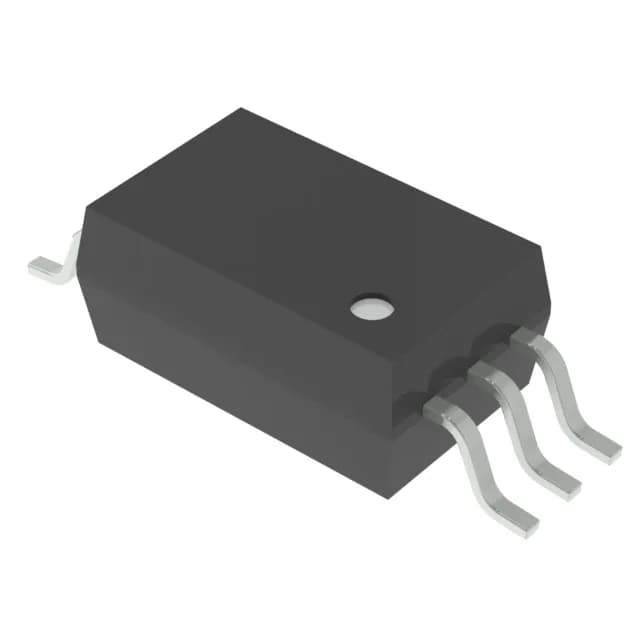
4 A peak output for high-capacitance IGBT/MOSFET gates
The Toshiba TLP5754(LF4,E is a single-channel gate-drive optocoupler that delivers a 4 A peak output current, sized to drive the gate capacitance of medium-power IGBTs and MOSFETs in inverter legs and motor drives. The 5000 Vrms isolation rating provides a reinforced safety barrier between the low-voltage controller side and the high-voltage power stage, while the 35 kV/µs common-mode transient immunity keeps the output state stable under the fast dv/dt edges that couple across the isolation gap in a hard-switched half-bridge. Rise and fall times of 15 ns and 8 ns respectively keep switching losses contained and let the designer budget dead-time margins without excessive guard-banding.
Supply rail and output drive
The output stage operates from a 15 V to 30 V supply rail, which covers the typical gate-drive voltages for IGBTs (15 V on, -5 V to -15 V off) and power MOSFETs (10 V to 15 V logic-level or standard). The part can source and sink 3 A symmetrically, so the gate charge is both pulled up and pulled down at the same rate — important for controlled turn-off and avoiding miller-plateau latch-up.
Propagation delay and timing budget
Maximum propagation delay is 150 ns in both directions, and the pulse-width distortion is capped at 50 ns. For a switching frequency of 20 kHz, that delay is about 0.3% of the period — negligible for most motor-drive and UPS designs, but worth checking in applications that need cycle-by-cycle current limiting or shoot-through prevention with very short blanking intervals. The 50 ns PWD spec means the on and off delays are matched closely, which simplifies dead-time calculation.
Package and approvals
It carries approvals from CQC, CSA, cUL, UL, and VDE, covering the major safety certifications for industrial and appliance power electronics.