Gate charge and switching speed — what the numbers mean for the driver
The TK2R4A08QM,S4X: Total gate charge is 179 nC at 10 V — this sets the drive current required for a given switching frequency. A gate driver sourcing 1 A charges the gate in roughly 180 ns, but the 13000 pF input capacitance at 40 V drain bias means the Miller plateau dominates the switching transition; the actual turn-on time depends on the driver's peak current and the gate-loop inductance. The recommended drive voltage range is 6 V to 10 V for achieving the rated Rds(on). At 6 V the on-resistance is higher than the 2.44 mOhm figure, so a 10 V rail is preferred for minimum conduction loss. The ±20 V Vgs max gives headroom for gate ringing in a hard-switched topology, but the absolute limit is tight — a snubber or gate resistor is advisable if the layout has more than 10 nH of common-source inductance.
Package and board integration — TO-220SIS through-hole
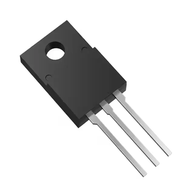
The TO-220SIS (supplier device package) is a fully isolated through-hole package — the metal tab is electrically isolated from the die, so no mica washer or sil-pad is needed between the device and the heatsink. This saves assembly time and reduces thermal resistance compared to a standard TO-220 with an insulator. The three leads are standard 0.025-inch thick, fitting a 1.6 mm PCB hole. Mounting torque on the screw should follow the package specification — typically 0.6 to 0.8 N·m for the TO-220SIS flange. Over-torquing cracks the epoxy body; under-torquing leaves an air gap that raises the junction-to-case thermal resistance above the 2.66 °C/W implied by the 47 W dissipation rating.