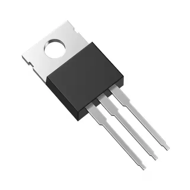
Toshiba Semiconductor TK155E65Z,S1X — Discrete Semiconductors

TK155E65Z,S1X Toshiba N-Ch MOSFET, 650V 18A TO-220

MPNTK155E65Z,S1X
End of Life

Toshiba Semiconductor TK155E65Z,S1X N-Channel MOSFET, DTMOS VI, 650 V, 18 A, 155 mOhm, TO-220-3, Tube.

$3.26Ref. price · indicative, final on quote
PackagingTO-220-3
RoHSROHS3 Compliant
Independent supplier — new & surplus stockAuthenticity-screened · ESD-safe packingListing updated Aug 2026

Specifications

TK155E65Z,S1X specifications
ParameterValue
FET typeN-Channel
MountingThrough Hole
Drain to source voltage650 V
Drive voltage (Max rds on, min rds on)10V
Current - continuous drain (Id) @ 25°C18A (Ta)
Power dissipation150W (Tc)
Operating temperature150°C
PackageTube
Vgs±30V
TechnologyMOSFET (Metal Oxide)
CaseTO-220-3
Vgs(th) (Max) @ id4V @ 730µA
Rds on (Max) @ id, vgs155mOhm @ 9A, 10V
Gate charge (Qg) (Max) @ vgs29 nC @ 10 V
Input capacitance (Ciss) (Max) @ vds1635 pF @ 300 V

Product details

650 V, 18 A, 155 mOhm — what these ratings mean for your switching load

The TK155E65Z,S1X: The 650 V drain-to-source breakdown voltage places it comfortably in the 400–600 V bus range common to PFC stages, flyback converters, and two-switch forward topologies — the voltage headroom above a 400 V rail covers switching transients and line surges without avalanche stress.

Total gate charge is 29 nC at 10 V, and input capacitance measures 1635 pF at 300 V drain bias. For a 100 kHz hard-switched converter, the gate driver must supply an average current of about 2.9 mA just to charge the gate — well within a standard 1 A driver, but the peak current at turn-on is set by the driver's source impedance and the gate resistance. The 29 nC figure also lets you estimate switching losses: each transition dissipates roughly 0.5 × Vds × Id × (tr + tf), and the gate charge determines how fast the Miller plateau is traversed.

TO-220 package — thermal and mechanical fit

The through-hole TO-220-3 package (supplier device package TO-220) dissipates up to 150 W at the case, but the real thermal limit depends on the heatsink and mounting torque. The 150 W figure is the absolute-maximum rating at Tc=25 °C; derate linearly above that case temperature per the datasheet's thermal resistance curve.

Frequently asked questions

What is the closest functional second-source to TK155E65Z,S1X?

The TK190E65Z,S1X is a parametric sibling in the same DTMOS VI family — same 650 V rating, same TO-220 package, but 190 mOhm Rds(on) at 7.5 A vs 155 mOhm at 9 A. It will drop into the same PCB footprint, but the higher on-resistance means higher conduction loss at the same load current. The TK110E65Z,S1X is the lower-Rds(on) sibling at 110 mOhm and 24 A. Neither is a pin-compatible second-source; each has its own gate charge and capacitance profile that may shift switching behavior.

What compliance documentation does Toshiba provide for TK155E65Z,S1X?

The TK155E65Z,S1X is ROHS3 compliant. No UL, IEC, or REACH documentation is listed in the available record.