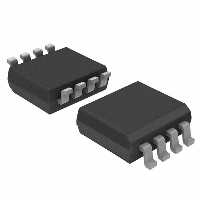
Toshiba Semiconductor TC75W55FK(TE85L,F) — Sensors & Transducers

TC75W55FK(TE85L,F) Dual CMOS Op-Amp – 160 kHz, 20 µA

MPNTC75W55FK(TE85L,F)
End of Life

Toshiba Semiconductor TC75W55FK(TE85L,F), dual CMOS operational amplifier, 160 kHz gain bandwidth, 20 µA supply per channel, 1.8 V to 7 V supply span, in 8-VFSOP (2.30 mm width) surface-mount package.

$0.63Ref. price · indicative, final on quote
Packaging8-VFSOP (0.091", 2.30mm Width)
RoHSRoHS Compliant
Sourced new & surplus through independent channelsAuthenticity-screened · ESD-safe packingListing updated Aug 2026

Specifications

TC75W55FK(TE85L,F) specifications
ParameterValue
MountingSurface Mount
Amplifier typeCMOS
Voltage - input offset2 mV
Voltage - supply span1.8 V
Current - supply20µA
Current - input bias1 pA
Operating temperature-40°C ~ 85°C
Gain bandwidth product160 kHz
PackageTape & Reel (TR); Cut Tape (CT)
Slew rate0.08V/µs
Case8-VFSOP (0.091\", 2.30mm Width)
Number of circuits2

Product details

Dual CMOS op-amp for low-power sensor signal conditioning

The TC75W55FK(TE85L,F): The TC75W55FK is a dual-channel CMOS operational amplifier from Toshiba, designed for battery-powered sensor interfaces and portable instrumentation where supply current is the primary constraint. Each amplifier draws 20 µA typical supply current, and the pair operates from a single supply rail between 1.8 V and 7 V.

The 160 kHz gain-bandwidth product sets the closed-loop bandwidth at a given gain: at gain 100, expect roughly 1.6 kHz of usable bandwidth. The 0.08 V/µs slew rate limits large-signal response — a 1 V step slews in about 12.5 µs, which is fine for DC measurement but too slow for audio or fast ADC driving. The picoamp-level bias makes the part suitable for high-impedance sources like pH probes or piezoelectric sensors without needing a separate JFET buffer. The 2 mV offset is typical for a general-purpose CMOS stage — budget for system calibration if the signal chain requires sub-millivolt accuracy.

The part is RoHS compliant. The 8-VFSOP package is a standard Toshiba footprint, and the supplier device package is 8-SSOP — the two designations refer to the same body outline, so PCB footprints are interchangeable.

8-VFSOP package — rework and footprint notes

The 8-VFSOP package measures 0.091" (2.30 mm) body width with a 0.50 mm lead pitch. The narrow pitch means the solder stencil apertures should be sized to avoid bridging — a 0.25 mm stencil thickness with 1:1 aperture-to-pad ratio is a safe starting point. Rework with hot air is feasible: the small thermal mass reflows quickly at 240–260 °C peak, but the fine pitch demands careful alignment.

Frequently asked questions

Where can I find the TC75W55FK datasheet PDF?

Design engineers need full specifications, pinout, and electrical characteristics to validate fit.

What is the current price and stock status of TC75W55FK?

Sourcing buyers need real-time pricing and availability to make procurement decisions.

Is TC75W55FK obsolete or still in production?

Buyers must confirm lifecycle status to avoid design-in risks or supply disruptions.

What are the equivalent or replacement parts for TC75W55FK?

When the exact part is unavailable, engineers and buyers need alternatives that match specs.

What is the pinout and package type of TC75W55FK?

Hardware designers need mechanical and pin compatibility for PCB layout.

Where can I buy TC75W55FK in cut tape or reel quantities?

Buyers need to know packaging options (TR, CT) to match assembly requirements.