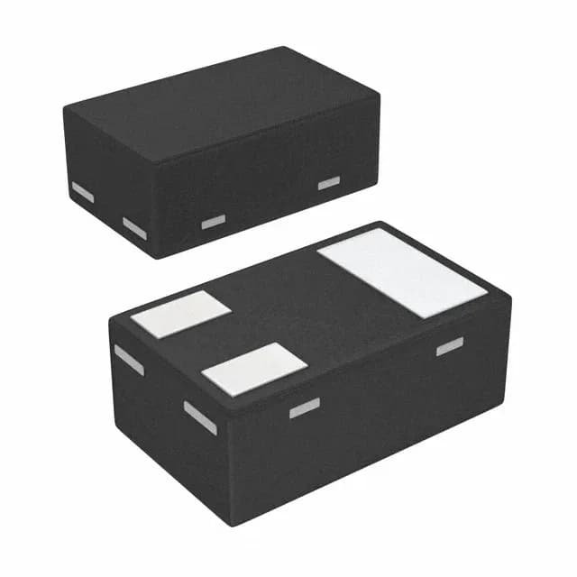
Toshiba Semiconductor SSM3K15ACTC,L3F

SSM3K15ACTC,L3F SSM3K15ACTC L3F MOSFET N-Ch 30V 100mA CST3C

MPNSSM3K15ACTC,L3F
End of Life

Toshiba U-MOSIII series, N-Channel MOSFET, 30 V drain-source, 100 mA continuous drain, 3.6 Ohm Rds(on) at 4 V drive, SC-101 / SOT-883 package, CST3C supplier device package.

$0.32Ref. price · indicative, final on quote
PackagingSC-101, SOT-883
StockContact for availability
MOQ1 pcs
  • 100% new & originalTraceable channels only — no refurbs, no pulls, no remarked parts.
  • Date & lot codes on quoteStated per line before you commit; label photos on request.
  • MSL-compliant ESD packingMoisture-sealed bags with indicator cards; reels photo-verified.
  • PayPal buyer protectionPay by T/T, PayPal or Payoneer — card payments covered end to end.

Specifications

SSM3K15ACTC,L3F Technical Specifications
ParameterValue
SeriesU-MOSIII
FET typeN-Channel
Mounting typeSurface Mount
Drain to source voltage30 V
Drive voltage (Max rds on, min rds on)2.5V, 4V
Current - continuous drain (Id) @ 25°C100mA (Ta)
Power dissipation500mW (Ta)
Operating temperature150°C
PackageTape & Reel (TR); Cut Tape (CT)
Vgs±20V
TechnologyMOSFET (Metal Oxide)
CaseSC-101, SOT-883
Vgs(th) (Max) @ id1.5V @ 100µA
Rds on (Max) @ id, vgs3.6Ohm @ 10mA, 4V
Input capacitance (Ciss) (Max) @ vds13.5 pF @ 3 V

Product details

30 V, 100 mA N-channel — signal-level load switch

The Toshiba SSM3K15ACTC,L3F is a small-signal N-channel MOSFET from the U-MOSIII series, rated for 30 V drain-to-source and 100 mA continuous drain current at 25 °C ambient. It is built for low-current load switching, level translation, and signal gating where board area is tight.

On-resistance and gate drive — 3.6 Ohm at 4 V

Maximum on-resistance is 3.6 Ohm at 10 mA drain current with a 4 V gate drive. The drive voltage range for minimum Rds(on) is 2.5 V to 4 V, meaning a 3.3 V logic GPIO can turn the MOSFET fully on without a level shifter. Input capacitance is only 13.5 pF at 3 V drain-source, so the gate charge per cycle is negligible. A microcontroller GPIO can drive the gate directly at moderate switching frequencies without an external driver.

Package and footprint — SC-101 / SOT-883 (CST3C)

The part is supplied in the SC-101 / SOT-883 package, with the supplier device package designated CST3C. This is a very small surface-mount package — the PCB footprint and solder-paste stencil aperture must be designed for the 0.50 mm pitch and small pad geometry typical of this case. Maximum power dissipation is 500 mW at 25 °C ambient, derated for higher temperatures. The junction temperature rating is 150 °C, consistent with the small package's thermal limits.

Active production — no obsolescence risk

For new designs, there is no last-time-buy pressure.

Frequently asked questions

What is the Rds(on) of SSM3K15ACTC?

At the minimum drive voltage of 2.5 V, Rds(on) is specified as the maximum value for that condition in the datasheet.

Is SSM3K15ACTC L3F RoHS compliant?

Yes, the part is ROHS3 compliant.

Is SSM3K15ACTC equivalent to SSM3K15ACT?

The suffix L3F typically indicates the packaging and reel specification (Tape & Reel). The die and electrical characteristics are the same as the base SSM3K15ACT. Confirm the exact suffix with the datasheet for ordering.

What is the maximum drain current for SSM3K15ACTC L3F?

The continuous drain current is 100 mA at 25 °C ambient temperature, rated for the SC-101 / SOT-883 package.

Can I drive the gate of SSM3K15ACTC L3F directly from a 3.3 V GPIO?

Yes. The drive voltage range for minimum on-resistance is 2.5 V to 4 V, and the gate threshold voltage is 1.5 V maximum at 100 µA. A 3.3 V logic output will fully enhance the MOSFET.