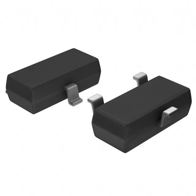
The internal bias network — a 4.7 kΩ base resistor (R1) in series with the base, and a 47 kΩ resistor (R2) between base and emitter — eliminates the two external resistors normally needed for a switching stage, saving board area and reducing pick-and-place cost on dense ECU, BCM, or sensor-interface PCBs. The 200 MHz transition frequency (fT) means this part can handle switching loads well into the low-MHz range — think CAN transceiver enable, solenoid pre-drive, or LED dimming PWM — without the base-drive overhead of a discrete transistor. The Vce(sat) maximum of 300 mV at 250 µA base current and 5 mA collector current gives a predictable on-state voltage drop for low-side switching. DC current gain (hFE) is a minimum of 80 at 10 mA collector current and 5 V Vce — typical for a pre-biased PNP, but the AEC-Q101 qualification means the gain and saturation limits are guaranteed across the automotive temperature range, not just at 25 °C.
It is not subject to a last-time-buy or end-of-life notice.
No special thermal pad or via stitching is needed at 200 mW; the standard FR-4 copper land pattern handles the dissipation.