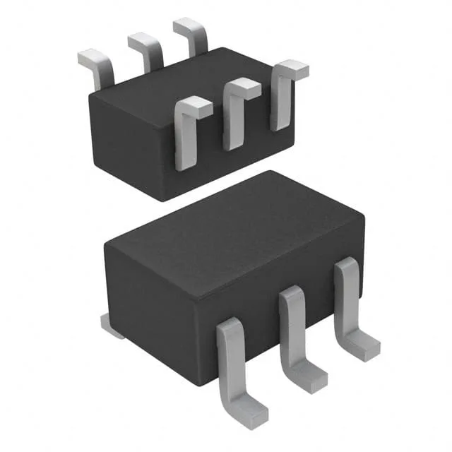
Dual-transistor array for compact biasing and signal switching
The HN1B01FU-GR,LF integrates one NPN and one PNP transistor in a single US6 (SOT-363) package, rated for 50 V collector-emitter breakdown and 150 mA continuous collector current per side. Minimum DC current gain of 200 at 2 mA, 6 V ensures consistent drive in low-current switching and amplifier stages where beta matching between the complementary pair matters.
Package and board-fit for high-density assembly
The 6-TSSOP, SC-88, SOT-363 footprint (supplier device package US6) is a standard 1.25 mm × 2.0 mm body with 0.65 mm lead pitch — it places without tombstoning on a standard reflow profile and shares land patterns with many dual-transistor parts.
Active lifecycle and compliance documentation
ROHS3 compliant per, with a maximum junction temperature rating of 125 °C, suiting it for consumer, industrial, and telecom environments where lead-free assembly and moderate ambient heat are standard.