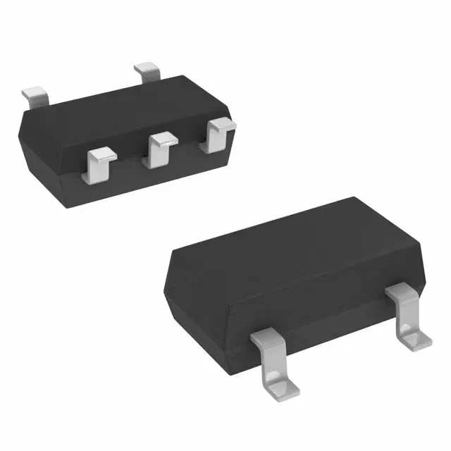
4.4 ns XOR gate for 3.3 V buses
Its 4.4 ns propagation delay at 3.3 V into 15 pF means it can keep up with a 100 MHz+ data path without adding a clock cycle of latency — useful for parity checking, address decoding, or glitch-free signal inversion on a mixed-voltage board. Outputs source and sink 8 mA each, enough to drive a standard CMOS input or a small LED directly.
The quiescent current maxes out at 1 µA, so it won't drain a battery rail in a parked system.
Input thresholds and supply tolerance
The low-level input threshold is 0.1 V to 0.4 V, and the high-level threshold is 2 V to 2.48 V — that's a clean 1.6 V noise margin on a 3.3 V rail.