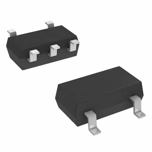
Toshiba Semiconductor 7UL1G00FU,LF — Logic ICs

7UL1G00FU,LF NAND Gate, 0.9V-3.6V, 4.4ns, SOT-353

MPN7UL1G00FU,LF
End of Life

Toshiba 7UL1G00FU,LF, single 2-input NAND gate, 0.9V–3.6V supply, 4.4ns propagation delay at 3.3V, 30pF, SOT-353 package, -40°C to 125°C, active.

$0.35Ref. price · indicative, final on quote
Packaging5-TSSOP, SC-70-5, SOT-353
RoHSROHS3 Compliant
Sourced new & surplus through independent channelsAuthenticity-screened · ESD-safe packingListing updated Jul 2026

Specifications

7UL1G00FU,LF specifications
ParameterValue
Logic typeNAND Gate
MountingSurface Mount
Voltage0.9V ~ 3.6V
Current - quiescent1 µA
Current - output high, low8mA, 8mA
I/O channels2
Operating temperature-40°C ~ 125°C
PackageTape & Reel (TR); Cut Tape (CT)
Case5-TSSOP, SC-70-5, SOT-353
Number of circuits1
Input logic level - low0.7V ~ 0.8V
Input logic level - high1.7V ~ 2V
Max propagation delay @ v, max CL4.4ns @ 3.3V, 30pF

Product details

Single 2-input NAND gate in a 5-pin SOT-353

The Toshiba 7UL1G00FU,LF is a single 2-input NAND gate in a tiny 5-pin SOT-353 package (also listed as 5-TSSOP / SC-70-5). The 1 µA quiescent current keeps the idle draw negligible.

4.4 ns propagation delay — fast enough for most glue logic

With a maximum propagation delay of 4.4 ns at 3.3 V with a 30 pF load, this gate handles clock gating, signal inversion, and enable decoding without adding a timing hazard. The 8 mA output drive (both high and low) is enough to fan out to a few CMOS loads or drive a short PCB trace.

The input logic thresholds scale with supply: low at 0.7V–0.8V, high at 1.7V–2V, so it cleanly interfaces with 1.8V and 3.3V logic families without extra level translation.

For a simple gate that fills a BOM line for years, this is the preferred lifecycle posture.

Frequently asked questions

What is the propagation delay of 7UL1G00FU?

Maximum propagation delay is 4.4 ns at 3.3V with a 30 pF load, fast enough for most glue-logic and level-translation tasks.

Can 7UL1G00FU be used as a replacement for 74LVC1G00?

Check the input threshold voltages and output drive against your specific design before substituting.