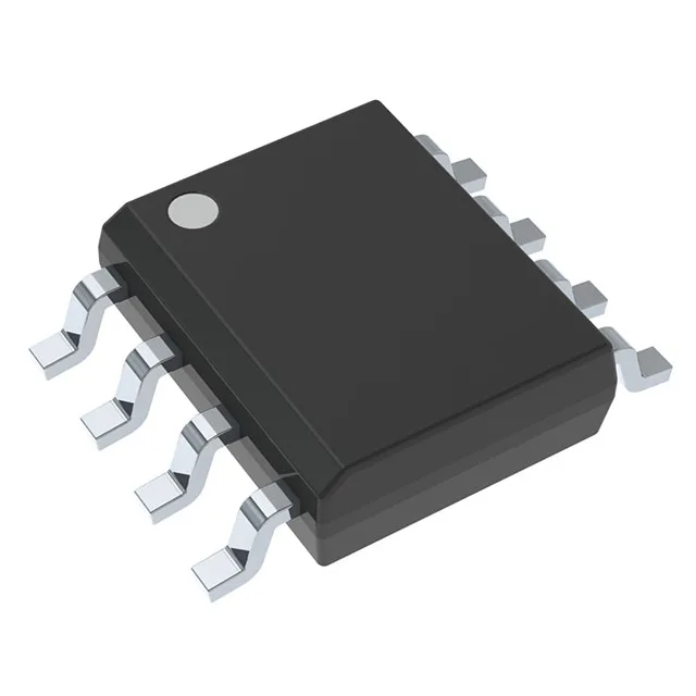
4.3 A peak, 75 ns propagation — the gate driver for SiC and IGBT switching
It delivers 4.3 A peak output current, with source/sink ratings of 2.4 A and 1.1 A respectively — enough to drive the gate charge of medium-power IGBTs and SiC MOSFETs in motor drives, inverters, and switched-mode power supplies.
100 kV/µs CMTI — why it matters for the inverter bus
In a half-bridge or full-bridge topology, the floating high-side gate driver sees the full DC-bus voltage swing at the switching node. A CMTI rating of 100 kV/µs means the UCC5310MCDR maintains data integrity across the isolation barrier even during hard-switching events — a spec that directly affects whether the gate signal glitches or the power device misfires. The 20 ns maximum pulse-width distortion (PWD) further limits timing asymmetry between turn-on and turn-off edges, which is critical for dead-time management in phase-leg designs.
Supply range and approvals
The output-side supply range spans 13.2 V to 33 V, covering the typical gate-drive voltages for IGBTs (15 V) and SiC MOSFETs (18–20 V). The input side is powered from the logic-side rail. The device carries approvals from CQC, CSA, UR, and VDE, which simplifies system-level certification for industrial and commercial power equipment.