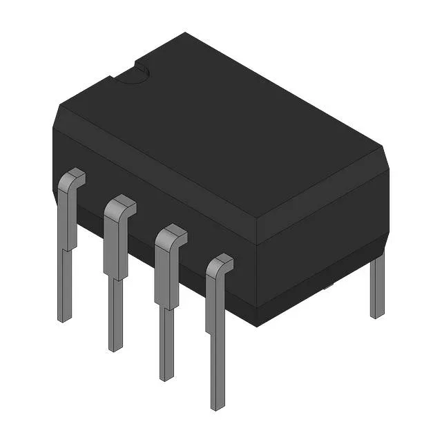
Dual 4 A peak low-side gate driver
Housed in a PDIP-8 package, it targets power-conversion stages where two independent gate-drive channels are needed — half-bridge primary-side drive, synchronous rectifier banks, or parallel MOSFET stages in DC-DC converters and motor-drive inverters. The high peak current reduces switching losses by charging the gate capacitance quickly, which is critical in high-frequency power supplies and class-D audio amplifiers.
The 4 A peak source/sink rating directly governs how fast the external FET's gate capacitance charges and discharges. A 10 nC gate-charge MOSFET transitions in roughly 2.5 ns at 4 A, which keeps the Miller plateau brief and the switching transition efficient. This matters for reducing cross-conduction in half-bridge topologies and for staying inside the FET's safe-operating area during hard-switching events. Designers sizing the bootstrap capacitor or the gate-drive transformer should budget for the full 4 A peak transient — the PDIP package's thermal impedance limits continuous duty, but the peak rating is the headline parameter for selecting this driver over a 2 A or 1 A alternative.
If a surface-mount variant is preferred, the same die is available in SOIC-8 (UCC37324D) — a straightforward footprint swap for reflow processes.
Where it fits in the power train
This driver sits between the PWM controller and the power FETs. Typical deployment includes isolated DC-DC converters, uninterruptible power supplies, motor-drive gate-drive boards, and class-D audio output stages. The non-inverting inputs simplify interface logic — one PWM signal per channel drives the corresponding FET directly. The PDIP-8 package suits prototype builds, low-volume production, and repair/rework environments where through-hole mounting is preferred over fine-pitch SMD.