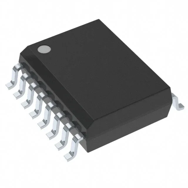
It drives two independent high-side or low-side switches, or a single half-bridge, with asymmetric peak output currents of 1.5 A (source) and 2.5 A (sink). The 40 ns maximum propagation delay and 6.5 ns maximum pulse-width distortion keep dead-time budgets tight for switching frequencies into the hundreds of kilohertz. Rise and fall times of 8 ns and 9 ns respectively reduce switching losses in IGBTs and SiC MOSFETs.
Asymmetric drive — why 1.5 A source and 2.5 A sink matter
The 1.5 A peak source current and 2.5 A peak sink current are not symmetric by accident. Many IGBT and SiC FET designs need a stronger pull-down to discharge the gate capacitance quickly during turn-off, reducing the Miller plateau duration and shoot-through risk. The UCC21541DW's sink-heavy drive matches that requirement without an external gate resistor split. If the load requires balanced source/sink, the 2.5 A sink channel can be paralleled with the 1.5 A source channel through a series resistor to equalise the gate charge profile.
Common-mode transient immunity — 100 V/ns for noisy environments
A minimum common-mode transient immunity of 100 V/ns ensures the output state does not glitch when the ground reference between primary and secondary bounces during hard-switching events. In a motor-drive or inverter stage where the switching node swings hundreds of volts in tens of nanoseconds, this rating is the margin that prevents false turn-on commands from reaching the power switch.