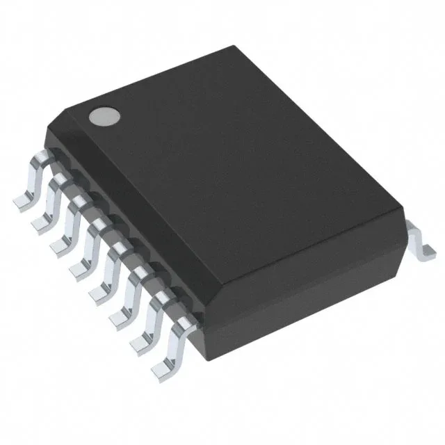
Texas Instruments UCC21520ADW — Digital Isolators

TI UCC21520ADW Isolated Gate Driver, 5.7 kVrms, 4A/6A

MPNUCC21520ADW
End of Life

Texas Instruments UCC21520ADW dual-channel isolated gate driver, capacitive coupling, 5700Vrms isolation, 4A source / 6A sink output, 30ns propagation delay, 16-SOIC package, -40°C to 125°C operating temperature.

$6.33Ref. price · indicative, final on quote
Packaging16-SOIC (0.295", 7.50mm Width)
StockContact for availability
MOQ1 pcs
  • 100% new & originalTraceable channels only — no refurbs, no pulls, no remarked parts.
  • Date & lot codes on quoteStated per line before you commit; label photos on request.
  • MSL-compliant ESD packingMoisture-sealed bags with indicator cards; reels photo-verified.
  • PayPal buyer protectionPay by T/T, PayPal or Payoneer — card payments covered end to end.

Specifications

UCC21520ADW Technical Specifications
ParameterValue
Mounting typeSurface Mount
Voltage - isolation5700Vrms
Voltage - output supply6.5V ~ 25V
Current - output high, low4A, 6A
Operating temperature-40°C ~ 125°C
Pulse width distortion6ns
Approval agencyCQC, CSA, UR, VDE
PackageTube
TechnologyCapacitive Coupling
Case16-SOIC (0.295\", 7.50mm Width)
Number of channels2
Rise (Fall time)6ns, 7ns
Propagation delay tpLH (tpHL)30ns, 30ns
Common mode transient immunity100V/ns

Product details

5.7 kVrms isolation, 4A/6A drive — what this gate driver is built for

The UCC21520ADW: It is designed to drive IGBTs, SiC MOSFETs, and GaN FETs in half-bridge, full-bridge, and multi-level converter topologies where the high-side switch floats on a fast-switching node. The 4A source and 6A sink output current charges the gate capacitance quickly enough for switching frequencies in the hundreds of kilohertz, while the matched 30ns maximum propagation delay on both channels simplifies dead-time management and reduces shoot-through risk in hard-switched bridges. The 100V/ns minimum common-mode transient immunity keeps the output state latched through the dv/dt of a SiC or GaN half-bridge switching event, which is the difference between a clean transition and a latch-up fault.

30 ns propagation delay — matched channels for balanced switching

Both channels share a 30ns maximum propagation delay, with pulse-width distortion max of 6ns.

16-SOIC footprint and supply range — layout and rail planning

The 16-SOIC (0.295", 7.50mm width) body with surface-mount termination is a common footprint shared by many TI isolated drivers, so a board layout for this part can often accommodate a pin-compatible alternate without a respin. The output supply range of 6.5V to 25V covers the typical gate-drive voltages for IGBTs (15V) and SiC MOSFETs (18V to 20V), and the 6.5V minimum is low enough to drive logic-level MOSFETs if the application needs it.

Approvals and compliance — CQC, CSA, UR, VDE

The UCC21520ADW carries approvals from CQC, CSA, UR, and VDE.

Frequently asked questions

Can UCC21520ADW drive SiC MOSFETs or GaN FETs?

Yes. The 4A source / 6A sink output is sufficient to drive the gate charge of most 600V to 1200V SiC MOSFETs and GaN HEMTs at switching frequencies up to several hundred kilohertz. The 100V/ns minimum CMTI ensures the output stays latched through the fast dv/dt of a SiC or GaN half-bridge switching node. The 6.5V to 25V output supply range covers the typical 18V to 20V gate-drive voltage for SiC FETs.