Half-bridge driver for synchronous N-channel bucks
It accepts a non-inverting input and delivers a 15 ns typical rise time and 10 ns fall time into the gate load, which sets the practical dead-time window for high-frequency switching. The 4.5 V to 5.5 V supply rail matches the bias from a typical PWM controller or a local 5 V regulator, so the BOM needs to budget that rail separately from the 12 V bootstrap supply for the high-side driver.
With a 15 ns rise and 10 ns fall, the driver can charge and discharge the MOSFET gate quickly enough to keep switching losses low at frequencies up to several hundred kilohertz. The asymmetry — faster fall than rise — is intentional for synchronous bucks: the low-side FET turns off faster to prevent cross-conduction during the dead-time interval. The logic input thresholds (VIL 0.7 V, VIH 4.0 V) are compatible with 5 V PWM controllers; they also accept 3.3 V logic if the high-level output of the controller exceeds 4.0 V, which some do not — check the controller's VOH against the 4.0 V VIH spec.
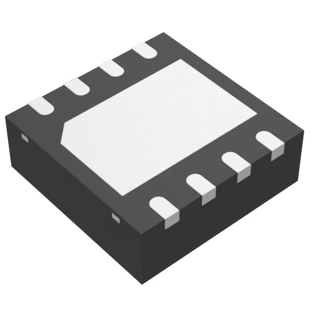
Package and thermal: 8-SON (3x3) with exposed pad
The TPS51601ADRBT comes in an 8-VDFN with exposed pad, also described as an 8-SON (3x3). Without that thermal via pattern, the junction temperature rises quickly above 400 mA continuous gate drive current.
No LTB risk, no forced redesign for a drop-in replacement.