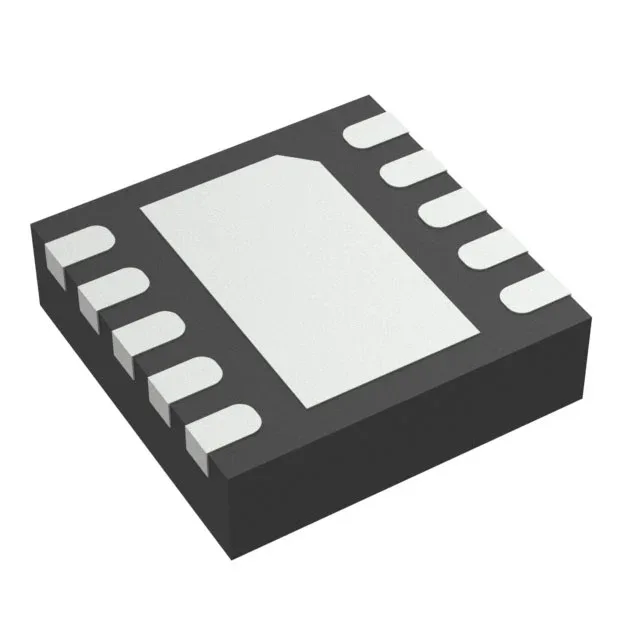
Texas Instruments TPS40305DRCR — Analog & Data Acquisition

TI TPS40305DRCR Buck Controller, 1.2MHz, 10-VSON

MPNTPS40305DRCR
End of Life

Texas Instruments TPS40305DRCR, step-down buck controller, 1.2MHz switching frequency, 3V–20V supply, synchronous rectification, 10-VSON (3x3) package, -40°C to 125°C junction temperature.

$2.57Ref. price · indicative, final on quote
Packaging10-VFDFN Exposed Pad
StockContact for availability
MOQ1 pcs
  • 100% new & originalTraceable channels only — no refurbs, no pulls, no remarked parts.
  • Date & lot codes on quoteStated per line before you commit; label photos on request.
  • MSL-compliant ESD packingMoisture-sealed bags with indicator cards; reels photo-verified.
  • PayPal buyer protectionPay by T/T, PayPal or Payoneer — card payments covered end to end.

Specifications

TPS40305DRCR Technical Specifications
ParameterValue
Output typeTransistor Driver
Mounting typeSurface Mount
Voltage - supply (Vcc (Vdd))3V ~ 20V
Frequency1.2MHz
Number of outputs1
Output phases1
Duty cycle85%
Operating temperature-40°C ~ 125°C (TJ)
PackageTape & Reel (TR); Cut Tape (CT)
FunctionStep-Down
TopologyBuck
Clock syncNo
Case10-VFDFN Exposed Pad
Control featuresEnable, Power Good, Soft Start
Output configurationPositive
Synchronous rectifierYes

Product details

What the TPS40305DRCR is and where it fits

The Texas Instruments TPS40305DRCR is a single-phase synchronous buck controller designed for step-down regulation from a 3V to 20V supply rail. It drives an external N-channel MOSFET pair and integrates synchronous rectification for higher efficiency at low output voltages — a common requirement in point-of-load (POL) converters for telecom, networking, and industrial equipment. The 1.2 MHz switching frequency lets you use smaller inductors and capacitors, shrinking the board footprint, but demands careful layout to keep switching noise out of sensitive analog sections. Control features include Enable, Power Good, and Soft Start, giving the designer sequenced start-up and fault reporting without extra glue logic.

1.2 MHz switching — what it means for the BOM

The 1.2 MHz switching rate is the headline parameter for the power-stage design. It pushes the inductor value down into the sub-microhenry range, which shrinks the magnetic component physically and reduces its DC resistance losses. The trade-off is higher switching losses in the FETs and tighter layout constraints to keep the switch node loop small. Plan for a low-ESR ceramic input capacitor close to the drain of the high-side FET and a ground plane under the controller to manage the di/dt edges. The 85% maximum duty cycle limits the step-down ratio at low input voltages — for a 3.3V output from a 5V rail the margin is comfortable, but from a 3.3V input you are near the ceiling.

Frequently asked questions

Is TPS40305DRCR lead-free and RoHS compliant?

Yes — the TPS40305DRCR is ROHS3 Compliant. The 10-VSON package is compatible with lead-free reflow profiles.