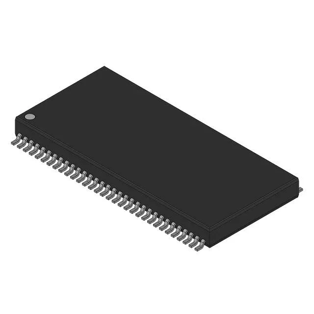
Texas Instruments TMS55161-70DGH — Analog & Data Acquisition

TMS55161-70DGH Video DRAM, 256Kx16, 70ns, PDSO64 – Active

MPNTMS55161-70DGH
End of Life

Texas Instruments TMS55161-70DGH, 256K x 16 Video DRAM, 70 ns access time, PDSO64 package, active lifecycle.

$7.0Ref. price · indicative, final on quote
StockContact for availability
MOQ1 pcs
  • 100% new & originalTraceable channels only — no refurbs, no pulls, no remarked parts.
  • Date & lot codes on quoteStated per line before you commit; label photos on request.
  • MSL-compliant ESD packingMoisture-sealed bags with indicator cards; reels photo-verified.
  • PayPal buyer protectionPay by T/T, PayPal or Payoneer — card payments covered end to end.

Specifications

TMS55161-70DGH Technical Specifications
ParameterValue
Series*
PackageBulk

Product details

70 ns access time — what it buys you in a frame buffer

The TMS55161-70DGH is a 256K by 16 video DRAM from Texas Instruments with a 70 ns access time, packaged in a PDSO64. This is the faster bin of the TMS55161 family, shaving 10 ns off the cycle compared to the 80 ns suffix variant. In a graphics frame buffer where the memory bus is the bottleneck, that 10 ns margin lets you tighten the pixel clock timing or run at a higher resolution without redesigning the controller logic. The 256Kx16 organization maps cleanly onto a 16-bit RGB or YUV data path — one chip covers one colour channel per pixel.

Active, but watch the lead-free constraint

No last-time-buy clock is ticking. However, the RoHS compliance flag is marked non-compliant, which means it uses tin-lead solder on the terminations — not the matte-tin finish you get on modern lead-free parts. If your assembly line is RoHS-exempt for legacy repair or military/aerospace work, this is fine. If you need lead-free for new EU-market equipment, you will need to source it under a waiver or look at a RoHS-compliant alternative.

PDSO64 — what you need for the footprint

The PDSO64 is a 64-pin plastic small-outline package, the standard VRAM footprint from that era. Pin pitch and body dimensions match the JEDEC MO-119 outline. If you are replacing a failed part on an existing board, the orientation is marked by pin 1 chamfer on the package body — no lab needed to figure out the orientation. For a new layout, the land pattern is the same as any other 64-pin TSOP-II memory, so the footprint is not exotic.

Frequently asked questions

How does TMS55161-70DGH compare to TMS55161-80DGH?

The only parametric difference between the two is the access time: 70 ns for the -70DGH versus 80 ns for the -80DGH. The -70DGH gives you a 10 ns faster cycle, which directly buys timing margin in the frame buffer controller. If your existing design uses the -80DGH and you have a few nanoseconds of slack, the -70DGH drops in as a straight speed upgrade — same package, same pinout, same density. If you are sourcing for a cost-sensitive build and the timing budget is comfortable, the -80DGH may be the cheaper option.