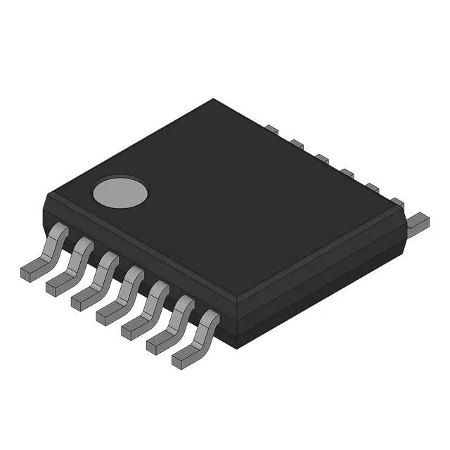
Texas Instruments TLV2784AIPW — Logic ICs

TLV2784AIPW Quad Op-Amp, 8 MHz GBW, 5V/µs Slew Rate

MPNTLV2784AIPW
End of Life

Texas Instruments TLV2784AIPW, quad general-purpose op-amp, 8 MHz gain bandwidth, 5V/µs slew rate, rail-to-rail output, 1.8 V to 3.6 V supply, –40°C to 125°C, 14-TSSOP package.

$0.87Ref. price · indicative, final on quote
Packaging14-TSSOP (0.173", 4.40mm Width)
StockContact for availability
MOQ1 pcs
  • 100% new & originalTraceable channels only — no refurbs, no pulls, no remarked parts.
  • Date & lot codes on quoteStated per line before you commit; label photos on request.
  • MSL-compliant ESD packingMoisture-sealed bags with indicator cards; reels photo-verified.
  • PayPal buyer protectionPay by T/T, PayPal or Payoneer — card payments covered end to end.

Specifications

TLV2784AIPW Technical Specifications
ParameterValue
Output typeRail-to-Rail
Mounting typeSurface Mount
Amplifier typeGeneral Purpose
Voltage - input offset250 µV
Voltage - supply span3.6 V
Current - supply650µA (x4 Channels)
Current - input bias2.5 pA
Current - output (Channel)23 mA
Operating temperature-40°C ~ 125°C
Gain bandwidth product8 MHz
PackageBulk
Slew rate5V/µs
Case14-TSSOP (0.173\", 4.40mm Width)
Number of circuits4

Product details

The 8 MHz gain-bandwidth product sets the usable closed-loop bandwidth: at a gain of 10, the –3 dB point lands near 800 kHz, which is adequate for audio-band anti-aliasing filters or 100 kHz sensor loops. The 5 V/µs slew rate means a full 2 V peak-to-peak output swing can settle in about 400 ns without slew-induced distortion, so the part handles fast pulse signals like those from a photodiode transimpedance stage without significant waveform degradation.

Low quiescent current and input bias for power-sensitive, high-impedance inputs

Total supply current is 650 µA for all four channels — about 162.5 µA per amplifier — which keeps the power budget tight in battery-operated multi-channel data acquisition systems. The 2.5 pA input bias current is low enough that a 1 MΩ source impedance introduces only 2.5 µV of voltage error, so the part can buffer high-impedance sensors like pH probes or piezoelectric accelerometers without a separate JFET buffer stage.

250 µV input offset — DC accuracy without trimming

The 250 µV maximum input offset voltage defines the DC error floor. For a gain of 100, that offset appears as 25 mV at the output, which is acceptable for many general-purpose measurement channels but may require calibration or a chopper-stabilized amplifier if sub-millivolt precision is needed. The rail-to-rail output can swing within a few millivolts of the supply rails, preserving headroom in low-voltage single-supply designs.

Active lifecycle, but RoHS non-compliant — plan your BOM accordingly

This restricts its use in markets that enforce RoHS exemptions (e.g., most consumer electronics sold in the EU). It remains acceptable for military, aerospace, medical, and certain industrial applications where leaded finishes are still permitted or exempt. If your BOM requires RoHS compliance, you will need to select a lead-free variant such as the TLV2784IDR or similar.

Frequently asked questions

What is the closest pin-compatible alternative to TLV2784AIPW?

A direct pin-compatible alternative is the TLV2784IDR, which offers the same quad general-purpose amplifier in a 14-SOIC package with similar electrical specs (8 MHz GBW, 5 V/µs slew rate, rail-to-rail output) but is RoHS compliant. Verify the package footprint difference (SOIC vs TSSOP) before substituting.

Where can I buy TLV2784AIPW?

The TLV2784AIPW is available to order through independent distribution.