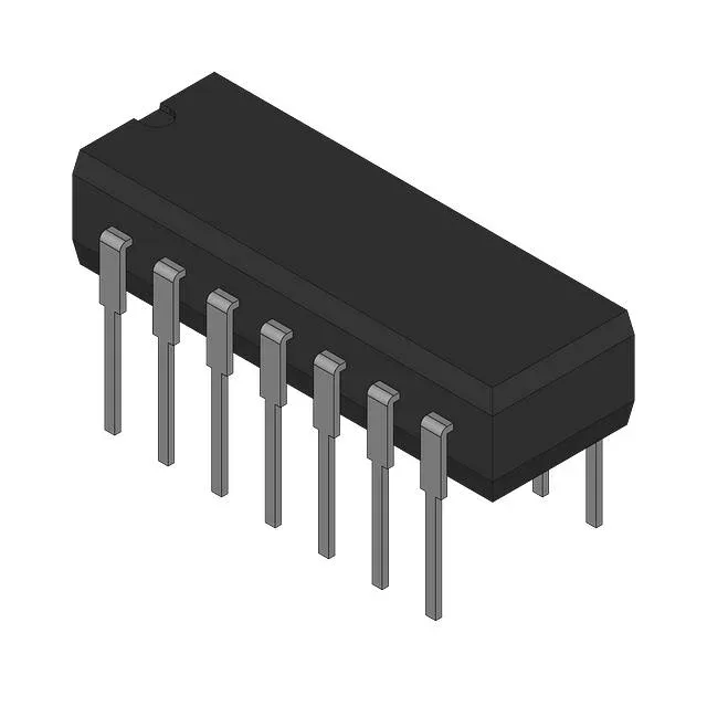
Dual op-amp with 9 MHz GBW and rail-to-rail output
This combination suits signal conditioning, active filters, and sensor interface circuits where moderate speed and single-supply operation are needed.
For a 5 V peak-to-peak signal, that supports full-power bandwidth up to roughly 318 kHz before slew-rate limiting distorts the waveform. This is faster than many general-purpose op-amps (e.g., the classic LM358 at 0.3 V/µs), making the TLV2633IN a better fit for higher-speed ADC drivers, pulse amplification, or waveform generation where the edge rate matters.
If the design sees sustained junction temperatures above 70°C ambient, check the derating curves or consider a wider-temperature variant.
Through-hole DIP — prototyping and legacy boards
The 14-DIP (0.300", 7.62mm) package with through-hole mounting is breadboard-friendly and easy to hand-solder. It is the right choice for lab prototypes, educational kits, or retrofitting existing through-hole PCB layouts. For high-density or automated assembly, surface-mount alternatives in the same family (e.g., TLV2633IDR in SOIC-8) are available, but the DIP version gives the rework tech a clear advantage during debug.