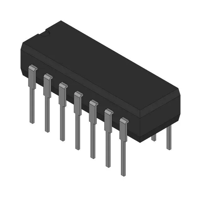
Hermetic JFET quad op-amp for harsh environments
The Texas Instruments TLE2074MJ is a JFET-input quad operational amplifier in a hermetic 14-CDIP ceramic package, designed for applications requiring wide temperature tolerance and high input impedance.
40 V/µs slew rate — why it matters for signal chain design
A 40 V/µs slew rate on a quad JFET op-amp is notably fast — most general-purpose quads sit around 10–20 V/µs. This means the TLE2074MJ can track a 10 V peak-to-peak sine wave up to roughly 630 kHz without significant slew-induced distortion, making it a candidate for driving the input of a high-speed ADC or for conditioning fast transient signals in a data acquisition front end. The 48 mA output current per channel gives it enough drive to handle moderate capacitive loads or multiple feedback paths without an external buffer.
14-CDIP hermetic package — sealed for mission-critical reliability
The 14-CDIP (0.300", 7.62mm) is a ceramic dual-in-line package with hermetic sealing, standard for high-reliability programs that require MIL-STD screening or JAN qualification. Unlike plastic SOIC or TSSOP packages, CDIP resists moisture ingress and outgassing, which is why it appears in satellite, missile guidance, and downhole instrumentation designs. The through-hole mounting suits legacy board layouts or sockets for field-replaceable modules.
Supply range and input characteristics
The TLE2074MJ operates from a single supply as low as 4.5 V up to a maximum of 38 V, or split supplies like ±2.25 V to ±19 V. This wide span covers standard industrial rails (5 V, ±15 V) and military bus voltages. Input bias current is 20 pA typical, which preserves accuracy when the source impedance is high — think photodiode amplifiers or precision integrators where pA-level leakage matters. Input offset voltage is 490 µV maximum, adequate for 12-bit systems with gain staging.
Because the package is through-hole and hermetic, the supply channel tends to be smaller-volume and order-driven compared to plastic surface-mount parts, so lead time should be verified during the BOM review cycle.