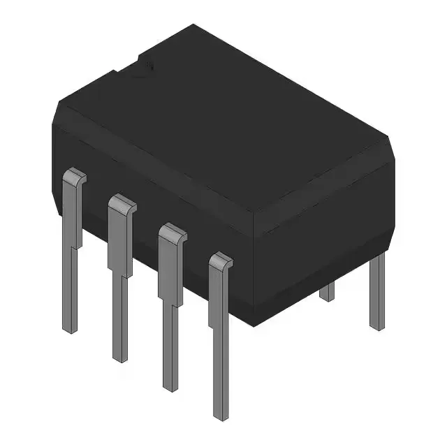
Dual JFET op-amp in a hermetic CDIP — built for the wide-temperature board
It delivers a 10 MHz gain-bandwidth product and a 45 V/µs slew rate, drawing 3.1 mA per channel from a supply spanning 4.5 V to 38 V. This is the part you specify when the board lives in an avionics bay, a satellite payload, or a downhole tool — environments where plastic packages and commercial temperature grades don't survive the qualification review.
The 45 V/µs slew rate means this op-amp can swing 10 V peak-to-peak at roughly 700 kHz without slewing into distortion — useful for conditioning fast sensor signals, driving ADC inputs, or active filtering in the audio band and above. The 10 MHz gain-bandwidth product gives you a closed-loop bandwidth of 1 MHz at a gain of 10, which covers most precision signal-chain needs. Paired with the 20 pA input bias current, the TLE2072AMJGB handles high-impedance sources like piezoelectric sensors or photodiode preamps without loading the signal. The 700 µV input offset voltage is typical for a JFET design at this speed — if you need lower offset, you'd step to a chopper-stabilized amplifier, but you'd give up the bandwidth and the wide supply range.
The 4.5 V minimum supply lets this op-amp run from a single 5 V rail alongside digital logic, while the 38 V maximum covers ±15 V split supplies or unregulated 24 V industrial buses. That range simplifies inventory — one qualified part number serves multiple board designs with different supply voltages. The 3.1 mA per channel quiescent current is moderate; on a dual-supply ±15 V rail, the total dissipation sits around 186 mW, well within the CDIP package's capability at 125°C ambient when you account for derating.
8-pin CDIP — the package that passes the high-rel review
The 8-CDIP (0.300", 7.62 mm) is a hermetic ceramic dual-in-line package with through-hole leads. This is the package you need when the specification calls for MIL-STD-883 or JAN screening, or when the board must withstand humidity, thermal cycling, and outgassing requirements that rule out plastic. The through-hole mounting is compatible with standard 0.100" pitch prototyping boards and socketed burn-in, but it does mean a larger footprint than a surface-mount SOIC — factor that into board area if you are retrofitting an existing design.
For a high-reliability program with a five- to ten-year production run, this removes the single-source obsolescence risk that often haunts ceramic-package parts.