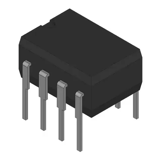
Hermetic JFET op-amp for harsh environments
The JFET input stage delivers an input bias current of 20 pA, preserving accuracy when interfacing with high-impedance sensors such as photodiodes, piezoelectric transducers, and precision strain-gauge bridges.
The TLE2071AMJGB operates from a single supply as low as 4.5 V or dual supplies up to ±19 V (38 V total span), making it compatible with 5 V logic rails and ±15 V industrial backplanes alike. Supply current is a moderate 1.6 mA per amplifier — not the lowest quiescent in the class, but a fair trade for the 10 MHz bandwidth and the hermetic package's thermal dissipation capability.
Package and mounting: ceramic DIP matters
Unlike plastic SOIC or DIP packages, CDIP resists moisture absorption, outgassing, and thermal cycling fatigue — the reason it appears in MIL-STD-883 and DESC-screened programs. The mounting type is through-hole, so board assembly requires wave soldering or a socket; no reflow profile for a plastic body applies. For a surface-mount alternative, see the FAQ on equivalent op-amps.