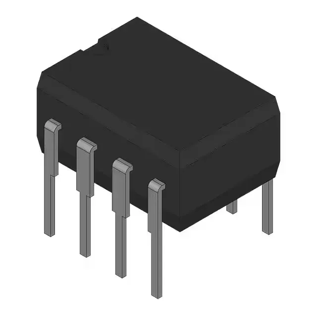
Texas Instruments TLE2062MJGB — Logic ICs

TLE2062MJGB JFET Op-Amp, 2 MHz, 3.4 V/µs, -55 to 125°C

MPNTLE2062MJGB
End of Life

Texas Instruments TLE2062MJGB, dual JFET-input operational amplifier, 2 MHz gain bandwidth, 3.4 V/µs slew rate, 7 V to 36 V supply, 8-CDIP package, -55°C to 125°C operating temperature.

$17.09Ref. price · indicative, final on quote
Packaging8-CDIP (0.300", 7.62mm)
StockContact for availability
MOQ1 pcs
  • 100% new & originalTraceable channels only — no refurbs, no pulls, no remarked parts.
  • Date & lot codes on quoteStated per line before you commit; label photos on request.
  • MSL-compliant ESD packingMoisture-sealed bags with indicator cards; reels photo-verified.
  • PayPal buyer protectionPay by T/T, PayPal or Payoneer — card payments covered end to end.

Specifications

TLE2062MJGB Technical Specifications
ParameterValue
Mounting typeThrough Hole
Amplifier typeJ-FET
Voltage - input offset900 µV
Voltage - supply span36 V
Current - supply625µA (x2 Channels)
Current - input bias4 pA
Current - output (Channel)80 mA
Operating temperature-55°C ~ 125°C (TA)
Gain bandwidth product2 MHz
PackageBulk
Slew rate3.4V/µs
Case8-CDIP (0.300\", 7.62mm)
Number of circuits2

Product details

Hermetic JFET op-amp for harsh environments

It combines a 2 MHz gain-bandwidth product with a 3.4 V/µs slew rate, drawing 625 µA per amplifier from a 7 V to 36 V supply.

The 2 MHz gain-bandwidth product and 3.4 V/µs slew rate are adequate for audio-frequency filtering, instrumentation amplifier stages, and control-loop compensation up to a few hundred kHz. The 4 pA input bias current (typical) preserves signal integrity in high-impedance sensor interfaces — photodiode amplifiers, pH probes, piezoelectric transducers — where a bipolar op-amp's nanoamp bias would swamp the signal. Input offset voltage is specified at 900 µV. For a JFET op-amp that is a moderate figure; designs requiring sub-500 µV offset should budget for trim or select a precision-grade alternative. The 7 V minimum supply span means this part does not run on a single 5 V rail — it needs at least ±3.5 V or a single supply above 7 V.

Package and temperature grade — design-in notes

The 8-CDIP package (0.300 inch body width, 7.62 mm) is a through-hole ceramic DIP. The through-hole mounting means the part is not a candidate for high-density SMT reflow assembly; it is socketed or hand-soldered into plated through-holes. The ceramic body also handles higher storage and operating temperatures than plastic, but the 125°C junction limit still governs derating — the 80 mA output current should be derated above 85°C ambient.

Frequently asked questions

What are the alternatives to TLE2062MJGB?

Within the same Excalibur JFET family, the TLE2062A (plastic DIP or SOIC) offers improved offset voltage but only a commercial/industrial temperature range. For a pin-compatible hermetic alternative, the OPA2132PA (8-PDIP) is plastic and stops at 85°C; no direct ceramic second source is listed. The closest functional peer in a hermetic package would be the OPA2111KM (8-TO-99 metal can), which is a single, not dual, op-amp.

Is TLE2062MJGB suitable for high-temperature applications?

Yes. This makes it suitable for engine bay electronics, downhole tools, and satellite payloads where ambient temperatures exceed 85°C.