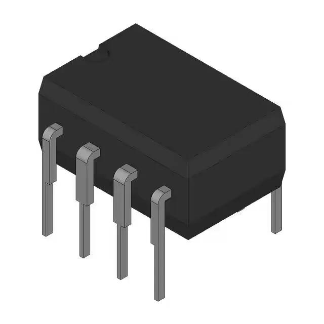
Dual differential comparator in a through-hole DIP
Each channel can sink or source up to 20 mA at the output, and the output stage is configurable as CMOS, MOS, open-drain, or TTL — so it can drive logic inputs, relay coils through a pull-up, or open-collector wired-OR buses without extra level shifters.
The TLC372IP runs on a single supply from 3 V to 16 V, or split supplies from ±1.5 V to ±8 V. That covers the common 5 V and 12 V industrial rails, plus 3.3 V logic systems with enough headroom for a 5 V-tolerant input stage. Quiescent current maxes out at 400 µA for both channels — low enough to leave the comparator biased continuously in a battery-powered sensor node without draining the pack overnight.
Input characteristics for high-impedance sensing
Input bias current is spec'd at 5 pA maximum at 5 V — a CMOS-input comparator that won't load a high-impedance source like a photodiode, pH probe, or high-value resistor divider.
The through-hole DIP package is forgiving in rework: a hot-air station or desoldering iron can lift it cleanly without lifting a pad, and the 0.300" body width fits standard breadboards and prototyping sockets.